The semiconductor industry is undergoing one of its most transformative shifts in decades. As demand for higher computing power, lower latency, and energy efficiency continues to surge, traditional chip design methods are reaching their physical and economic limits. Enter the chiplet ecosystem a new approach that champions modularity, scalability, and above all, collaboration.
The Rise of Chiplet Architecture
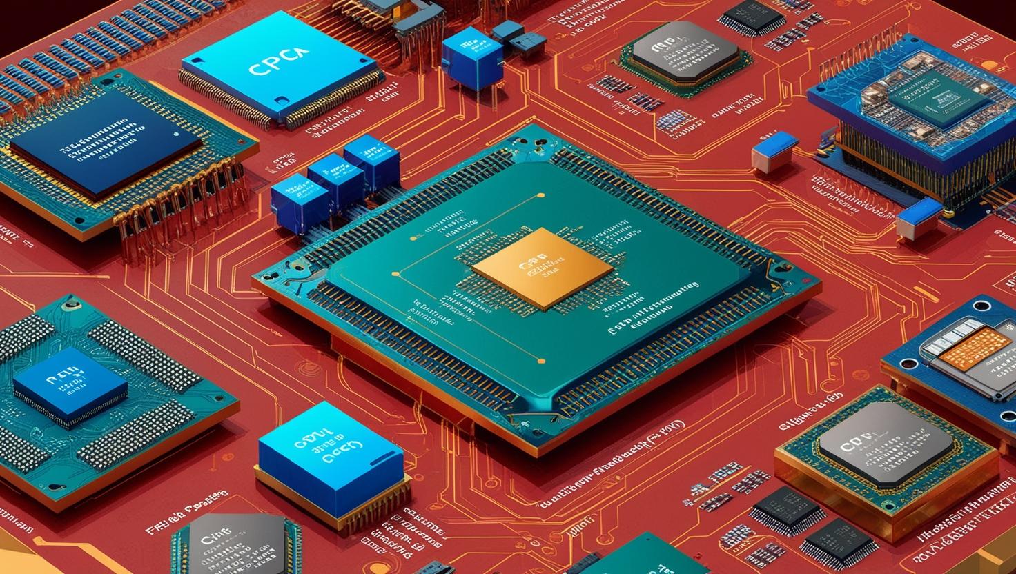
In the past, chipmakers relied heavily on monolithic chip design, where all components were integrated into a single piece of silicon. While this approach dominated for years, it became increasingly difficult to scale as transistor density grew and fabrication costs soared. Chiplets have emerged as the answer to these challenges.
A chiplet is a smaller, specialized piece of silicon that performs a specific function, such as processing, graphics, or I/O management. Instead of designing one large chip, manufacturers can now integrate multiple chiplets into a single package. This modular architecture offers significant advantages: it allows companies to reuse proven designs, improve manufacturing yields, and accelerate time-to-market for new products. In essence, chiplets enable a “Lego-like” approach to chip design, where different blocks can be assembled to create custom solutions for diverse applications.
Collaboration as the Foundation of Progress
The chiplet revolution cannot thrive in isolation. Its success depends on a broad ecosystem of collaboration among semiconductor designers, foundries, packaging companies, and electronic design automation (EDA) tool providers. Unlike traditional chip development, where a single company could control the entire design and manufacturing process, chiplets introduce an environment where interoperability is key.
To achieve this, the industry is working toward standardized communication interfaces that allow chiplets from different vendors to operate together seamlessly. One of the most notable initiatives in this space is Universal Chiplet Interconnect Express (UCIe), a consortium-driven standard that defines protocols for data exchange between chiplets. This effort marks a significant step toward open innovation, enabling companies to combine best-in-class chiplets from multiple suppliers without compromising on performance, power efficiency, or reliability.
Download PDF Brochure @ https://www.marketsandmarkets.com/pdfdownloadNew.asp?id=131809383
The Economic and Technical Advantages
Chiplet-based design offers both economic and technical advantages that are hard to ignore. Smaller dies are easier and cheaper to manufacture than large monolithic chips, which are more prone to defects. This leads to better yield rates and lower production costs. Moreover, chiplet modularity allows companies to scale computing power simply by adding or upgrading specific chiplets, rather than redesigning an entire processor.
From a performance perspective, chiplets enable greater design flexibility. Engineers can mix different process technologies—such as combining high-performance logic on advanced nodes with memory or analog components on mature ones—within a single package. This heterogeneous integration optimizes performance while controlling costs, a key advantage as the industry continues to move beyond Moore’s Law.
Expanding Applications Across Industries
The adoption of chiplet technology is accelerating across multiple sectors. In artificial intelligence and machine learning, chiplets allow for modular compute units that can be scaled to handle increasingly complex workloads. High-performance computing (HPC) environments benefit from the ability to integrate multiple processors in one package, delivering unparalleled speed for research, simulation, and data analytics.
In 5G communications and networking, chiplets enhance signal processing and power management, ensuring faster data transfer and reduced latency. Even consumer electronics are beginning to embrace chiplet-based designs, leveraging their efficiency to build thinner, lighter, and more powerful devices. The versatility of this approach allows manufacturers to tailor hardware to specific market demands without the long design cycles of traditional chips.
Challenges and the Path Forward
While the benefits of chiplets are compelling, the ecosystem still faces challenges that require collective effort. Standardization, thermal management, and cross-vendor interoperability remain complex issues that the industry must continue to refine. The ability to effectively design, assemble, and test multi-chip packages at scale will determine how quickly chiplets become the new norm.
Nonetheless, the momentum is undeniable. The convergence of open standards, advanced packaging techniques, and collaborative innovation is setting the stage for a new era in semiconductor design. The future of chip development is no longer about who can make the smallest transistors—it’s about who can build the smartest systems through partnership and integration.
A Collaborative Future
The chiplet ecosystem represents more than a technological evolution; it symbolizes a cultural shift in the semiconductor industry. For decades, innovation was driven by competition and proprietary advancement. Today, progress hinges on openness, shared standards, and collective expertise. As chiplet architectures mature, collaboration will not only drive efficiency but also unlock new possibilities across computing, connectivity, and intelligence.
The semiconductor industry’s next leap forward will be built—not by a single company—but by an entire ecosystem working together to redefine what’s possible in the world of silicon.
Chiplets are more than just a new way to build chips; they are the foundation of a new era in semiconductor innovation—one powered by collaboration, modular design, and shared technological progress. The journey ahead is complex, but the future of computing has never looked more connected.
Industry FAQ
1. What is a chiplet?
A chiplet is a small, functional block of silicon designed to perform a specific task within a larger integrated circuit (IC) system. Instead of manufacturing one large monolithic chip, multiple chiplets can be combined within a single package to create a complete system-on-chip (SoC).
2. How is a chiplet different from a traditional monolithic chip?
Traditional chips integrate all functions on a single piece of silicon. Chiplet-based designs, by contrast, disaggregate those functions across multiple smaller dies (chiplets). These are interconnected within one package using high-speed interfaces or advanced packaging technologies.
Benefits include:
- Higher yield and lower cost (smaller dies are easier to manufacture)
- Design flexibility and modularity
- Ability to mix and match technologies (e.g., logic, memory, analog, I/O)
- Faster time-to-market through reuse of existing chiplets
3. Why is the chiplet approach gaining popularity now?
The chiplet trend is driven by:
- Rising costs of advanced nodes (e.g., 5nm, 3nm)
- Yield challenges with large monolithic dies
- Heterogeneous integration needs, combining analog, digital, and memory in one package
- Performance gains enabled by advanced packaging and interconnect standards such as UCIe (Universal Chiplet Interconnect Express)