The semiconductor industry is entering a new phase—one where performance gains are no longer driven solely by shrinking transistors, but by how intelligently chips are connected and integrated. At the forefront of this transformation is hybrid bonding, a technology that is quietly reshaping the architecture of next-generation devices. From artificial intelligence to advanced memory systems, hybrid bonding is emerging as a critical enabler of faster, more efficient, and highly compact semiconductor solutions.
The global hybrid bonding market is projected to reach USD 633.9 million by 2032 from USD 164.7 million in 2025, registering a CAGR of 21.2% from 2025 to 2032
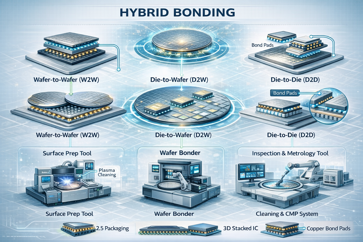
Rethinking Chip Design in the Post-Scaling Era
For decades, the industry relied on continuous transistor miniaturization to improve performance. Today, physical and economic constraints have slowed that progress. As a result, chipmakers are rethinking design strategies—shifting toward 3D integration and heterogeneous architectures.
Hybrid bonding fits perfectly into this new paradigm. By enabling direct connections between chips at the atomic level—without the need for traditional solder bumps—it allows multiple components to function almost as a single unified system. This opens the door to entirely new chip designs that were previously impractical or impossible.
What Makes Hybrid Bonding Different?
Unlike conventional interconnect technologies, hybrid bonding simultaneously connects both the metal interconnects and dielectric surfaces of two wafers or dies. This results in:
- Ultra-fine pitch interconnections
- Minimal electrical resistance and signal loss
- Improved thermal and mechanical stability
- Higher interconnect density compared to micro-bumping
- The outcome is a dramatic improvement in speed, bandwidth, and energy efficiency, all of which are essential for modern computing workloads.
Download PDF Brochure @ https://www.marketsandmarkets.com/pdfdownloadNew.asp?id=2641237
Fueling the Next Wave of Innovation
Hybrid bonding is not just an incremental improvement—it is a foundational technology enabling several major industry trends:
1. AI and High-Performance Computing
Modern AI models demand immense computational power and rapid data movement. Hybrid bonding allows processors and memory to be stacked closely together, reducing latency and increasing throughput. This tight integration is key to accelerating machine learning and data analytics.
2. Advanced Memory Architectures
Memory technologies such as high-bandwidth memory (HBM) are evolving rapidly. Hybrid bonding enables dense vertical stacking, allowing more memory layers to be integrated within a smaller footprint while maintaining high performance.
3. Chiplet Ecosystems
The shift toward chiplet-based design is redefining semiconductor manufacturing. Instead of building a single monolithic chip, manufacturers can combine smaller, specialized dies. Hybrid bonding ensures these chiplets communicate seamlessly, effectively functioning as one cohesive unit.
4. Edge and Consumer Electronics
As devices become smarter and more compact, there is growing demand for solutions that deliver high performance with low power consumption. Hybrid bonding supports this by reducing energy loss and enabling compact form factors.
Industry Momentum and Strategic Importance
Hybrid bonding is rapidly gaining traction across the semiconductor ecosystem. Leading chip manufacturers and equipment providers are investing heavily in scaling the technology for high-volume production. It is increasingly being integrated into long-term roadmaps for advanced packaging and 3D IC development.
What makes hybrid bonding particularly strategic is its ability to extend the life of existing semiconductor nodes. Instead of relying solely on costly node transitions, companies can achieve performance gains through smarter integration, improving return on investment.
Challenges on the Path to Scale
Despite its advantages, hybrid bonding is not without obstacles:
Precision manufacturing: Aligning wafers at extremely fine scales requires advanced equipment and process control
Cost barriers: Initial investment in tools and infrastructure is high
Thermal management: As chips are stacked more densely, dissipating heat becomes increasingly complex
Yield optimization: Ensuring defect-free bonding at scale remains a technical challenge
Overcoming these hurdles will require continued innovation in materials, process engineering, and system design.
The Road Ahead
Looking forward, hybrid bonding is expected to evolve from a cutting-edge innovation into a mainstream manufacturing standard. As the demand for computing power continues to surge—driven by AI, cloud computing, and connected devices—the need for efficient, high-density integration will only grow stronger.
Future developments may include:
Integration of diverse materials and functionalities within a single package
Further reduction in interconnect pitch for even higher density
Greater adoption in automotive, healthcare, and IoT applications
Fully automated, high-throughput hybrid bonding production lines
Hybrid bonding represents a turning point in semiconductor innovation. By enabling unprecedented levels of integration, performance, and efficiency, it is redefining how chips are designed and built. As the industry moves beyond traditional scaling limits, this technology will play a central role in powering the next generation of digital advancements.
In a world increasingly driven by data and intelligent systems, hybrid bonding is not just a technical upgrade—it is a cornerstone of the future semiconductor landscape.
FAQs: Future of Hybrid Bonding Market
1. What is hybrid bonding in semiconductors?
Hybrid bonding is an advanced packaging technology that directly connects two semiconductor wafers or dies using both metal (copper) and dielectric layers. It eliminates the need for traditional solder bumps, enabling faster, denser, and more energy-efficient interconnections.
2. Why is hybrid bonding important for next-generation chips?
Hybrid bonding enables higher bandwidth, lower latency, and improved power efficiency. These benefits are essential for modern applications like artificial intelligence (AI), high-performance computing (HPC), and advanced memory systems.
3. How does hybrid bonding differ from traditional packaging methods?
Traditional methods use micro-bumps to connect chips, which limit interconnect density and increase resistance. Hybrid bonding offers:
Much finer interconnect pitch
Better electrical performance
Lower power consumption
Greater scalability for 3D integration
4. What industries benefit the most from hybrid bonding?
Hybrid bonding is widely used in:
AI and data centers
Consumer electronics (smartphones, wearables)
Automotive electronics (ADAS, EV systems)
Telecommunications (5G/6G infrastructure)
About MarketsandMarkets™
MarketsandMarkets™ has been recognized as one of America’s Best Management Consulting Firms by Forbes, as per their recent report.
MarketsandMarkets™ is a blue ocean alternative in growth consulting and program management, leveraging a man-machine offering to drive supernormal growth for progressive organizations in the B2B space. With the widest lens on emerging technologies, we are proficient in co-creating supernormal growth for clients across the globe.
Today, 80% of Fortune 2000 companies rely on MarketsandMarkets, and 90 of the top 100 companies in each sector trust us to accelerate their revenue growth. With a global clientele of over 13,000 organizations, we help businesses thrive in a disruptive ecosystem.
The B2B economy is witnessing the emergence of $25 trillion in new revenue streams that are replacing existing ones within this decade. We work with clients on growth programs, helping them monetize this $25 trillion opportunity through our service lines – TAM Expansion, Go-to-Market (GTM) Strategy to Execution, Market Share Gain, Account Enablement, and Thought Leadership Marketing.
Built on the ‘GIVE Growth’ principle, we collaborate with several Forbes Global 2000 B2B companies to keep them future-ready. Our insights and strategies are powered by industry experts, cutting-edge AI, and our Market Intelligence Cloud, KnowledgeStore™, which integrates research and provides ecosystem-wide visibility into revenue shifts.
To find out more, visit www.MarketsandMarkets™.com or follow us on Twitter , LinkedIn and Facebook .
Contact:
Mr. Rohan Salgarkar
MarketsandMarkets™ INC.
1615 South Congress Ave.
Suite 103, Delray Beach, FL 33445
USA: +1-888-600-6441