The semiconductor industry is entering a new phase of innovation—one where performance gains are no longer driven solely by shrinking transistors, but by how intelligently chips are integrated. At the heart of this shift is hybrid bonding, a breakthrough technology that is rapidly gaining traction as demand rises for faster, more efficient, and highly compact semiconductor devices. The global hybrid bonding market is projected to reach USD 633.9 million by 2032 from USD 164.7 million in 2025, registering a CAGR of 21.2% from 2025 to 2032
A Turning Point in Chip Integration
For decades, Moore’s Law guided the industry’s progress. Today, as physical scaling approaches its limits, manufacturers are rethinking how chips are designed and assembled. Hybrid bonding is emerging as a key solution, enabling direct electrical and mechanical connections between wafers or dies without the need for traditional interconnect structures like micro-bumps.
This approach allows for:
- Significantly higher interconnect density
- Reduced power consumption
- Improved signal performance
- Greater design flexibility
In simple terms, hybrid bonding is helping transform chips into highly integrated systems, rather than isolated components.
Why the Market is Gaining Momentum
The rapid acceleration of the hybrid bonding market is closely tied to several macro technology trends:
1. AI and Data-Intensive Workloads
Artificial intelligence, machine learning, and high-performance computing are pushing current architectures to their limits. Hybrid bonding enables tighter integration between logic and memory, reducing latency and dramatically improving processing efficiency.
2. Rise of Chiplet Architectures
Instead of building a single monolithic chip, manufacturers are now designing modular “chiplets” that can be combined into a single package. Hybrid bonding provides the ultra-precise connections needed to make these architectures viable at scale.
3. Demand for Advanced Memory Solutions
Technologies like high-bandwidth memory (HBM) rely on vertical stacking and dense interconnects—areas where hybrid bonding excels.
4. Growth in Advanced Packaging
As packaging becomes as important as the chip itself, hybrid bonding is becoming a cornerstone of next-generation packaging strategies.
Download PDF Brochure @ https://www.marketsandmarkets.com/pdfdownloadNew.asp?id=2641237
Expanding Applications Across Industries
Hybrid bonding is not limited to one segment—it is influencing multiple areas of the semiconductor ecosystem:
Data centers: Enabling faster AI model training and inference
Consumer electronics: Supporting compact, high-performance devices
Automotive: Powering advanced driver-assistance systems (ADAS) and autonomous technologies
Healthcare & imaging: Enhancing sensor performance and miniaturization
Its versatility is one of the key reasons the market is expanding so rapidly.
Challenges on the Path to Scale
Despite its promise, hybrid bonding is not without complexities. The technology requires:
- Extremely clean and controlled manufacturing environments
- Ultra-high alignment precision at the nanoscale
- Significant capital investment in advanced equipment
In addition, achieving consistent yields at high volumes remains a technical challenge for many manufacturers.
Regional and Competitive Landscape
Global semiconductor leaders—especially in Asia-Pacific and North America—are investing heavily in hybrid bonding capabilities. Foundries, integrated device manufacturers (IDMs), and equipment suppliers are all racing to develop scalable solutions and establish leadership in this emerging space.
Strategic partnerships and ecosystem collaboration are becoming critical, as no single player can fully unlock the potential of hybrid bonding alone.
The Road Ahead
Looking forward, hybrid bonding is expected to play a central role in enabling:
- 3D integrated circuits (3D ICs)
- Heterogeneous integration across different process nodes
- Next-generation AI accelerators
- Energy-efficient computing architectures
As digital transformation accelerates across industries, the need for more powerful yet efficient chips will only intensify—and hybrid bonding is uniquely positioned to meet that demand.
Final Thoughts
The evolution of semiconductors is no longer just about making things smaller—it’s about making them smarter, faster, and more interconnected. Hybrid bonding represents a fundamental shift in how chips are built and integrated.
As next-generation applications continue to push the boundaries of performance, this technology is set to move from a niche innovation to a mainstream manufacturing standard.
Key companies operating in the hybrid bonding market include EV Group (EVG) (Austria), Applied Materials, Inc. (US), SUSS MicroTec SE (Germany), Besi (Netherlands), Kulicke & Soffa Industries, Inc. (Singapore), Tokyo Electron (TEL) (Japan), and ASMPT (Singapore), among others.
FAQ
What is hybrid bonding in semiconductors?
Hybrid bonding is an advanced semiconductor packaging technology that enables direct bonding of copper-to-copper and dielectric-to-dielectric surfaces without using traditional micro-bumps, allowing for higher interconnect density and improved performance.
Why is hybrid bonding important for next-generation chips?
Hybrid bonding supports 3D integration and chiplet architectures, enabling faster data transfer, lower power consumption, and better overall efficiency—critical for AI, HPC, and advanced memory applications.
What are the key drivers of the hybrid bonding market?
Major growth drivers include:
- Rising demand for AI and high-performance computing
- Increasing adoption of 3D ICs and chiplets
- Growth in advanced memory technologies (e.g., HBM)
- Expansion of advanced semiconductor packaging
Which industries benefit the most from hybrid bonding?
Hybrid bonding is widely used across:
Data centers and cloud computing
Consumer electronics
Automotive (ADAS and autonomous systems)
Healthcare and imaging technologies
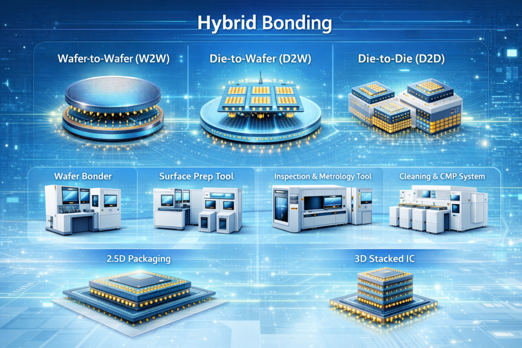
What are the main types of hybrid bonding?
The two primary types include:
Die-to-Die (D2D) Bonding – Used in chiplet-based designs
Wafer-to-Wafer (W2W) Bonding – Suitable for high-volume manufacturing
What challenges does the hybrid bonding market face?
Key challenges include:
High equipment and implementation costs
Complex manufacturing processes
Stringent cleanliness and alignment requirements
Yield and scalability concerns
Which regions are leading in hybrid bonding adoption?
Asia-Pacific leads the market due to strong semiconductor manufacturing ecosystems, followed by North America and Europe with significant R&D investments.
How does hybrid bonding compare to traditional packaging methods?
Compared to traditional methods, hybrid bonding offers:
- Higher interconnect density
- Lower latency and power consumption
- Better performance scalability
- Smaller form factors
About MarketsandMarkets™
MarketsandMarkets™ has been recognized as one of America’s Best Management Consulting Firms by Forbes, as per their recent report.
MarketsandMarkets™ is a blue ocean alternative in growth consulting and program management, leveraging a man-machine offering to drive supernormal growth for progressive organizations in the B2B space. With the widest lens on emerging technologies, we are proficient in co-creating supernormal growth for clients across the globe.
Today, 80% of Fortune 2000 companies rely on MarketsandMarkets, and 90 of the top 100 companies in each sector trust us to accelerate their revenue growth. With a global clientele of over 13,000 organizations, we help businesses thrive in a disruptive ecosystem.
The B2B economy is witnessing the emergence of $25 trillion in new revenue streams that are replacing existing ones within this decade. We work with clients on growth programs, helping them monetize this $25 trillion opportunity through our service lines – TAM Expansion, Go-to-Market (GTM) Strategy to Execution, Market Share Gain, Account Enablement, and Thought Leadership Marketing.
Built on the ‘GIVE Growth’ principle, we collaborate with several Forbes Global 2000 B2B companies to keep them future-ready. Our insights and strategies are powered by industry experts, cutting-edge AI, and our Market Intelligence Cloud, KnowledgeStore™, which integrates research and provides ecosystem-wide visibility into revenue shifts.
To find out more, visit www.MarketsandMarkets™.com or follow us on Twitter , LinkedIn and Facebook .
Contact:
Mr. Rohan Salgarkar
MarketsandMarkets™ INC.
1615 South Congress Ave.
Suite 103, Delray Beach, FL 33445
USA: +1-888-600-6441