The semiconductor industry is undergoing a fundamental architectural shift. As traditional monolithic chip scaling faces physical, economic, and thermal limitations, chiplet-based design has emerged as a scalable alternative. The chiplet ecosystem is rapidly evolving, driven by advances in advanced packaging technologies, heterogeneous integration, and the explosive demand for AI and high-performance computing (HPC).
The chiplet market is expected to grow from USD 51.94 billion in 2025 to USD 157.23 billion by 2030, at a CAGR of 24.8% during the forecast period. fueled largely by AI workloads and advanced packaging innovations.
At the center of this transformation lies a new design philosophy: instead of building a single large system-on-chip (SoC), semiconductor companies are increasingly combining smaller functional blocks—chiplets—within a single advanced package. This shift is reshaping the entire value chain, from design and fabrication to packaging and system integration.
1. The Rise of the Chiplet Ecosystem
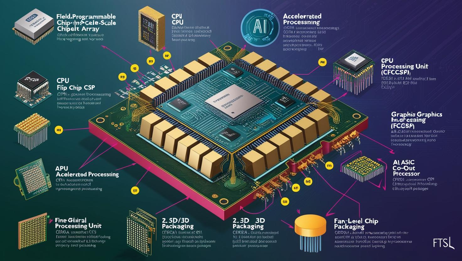
Chiplets are modular semiconductor components that perform specific functions such as compute, I/O, memory, or acceleration. These chiplets are integrated within a single package using advanced interconnect technologies.
The growing adoption of chiplets is driven by a combination of performance, cost, and scalability advantages. As process nodes shrink below 5nm, the cost of designing and manufacturing monolithic chips has increased dramatically, often reaching hundreds of millions or even billions of dollars per design cycle. Chiplets offer an alternative by breaking large chips into smaller, reusable building blocks, reducing both risk and cost.
Industry research highlights that chiplet architectures enable up to 30% cost reduction compared to traditional monolithic designs while improving yield by isolating defects to individual dies rather than entire wafers.
This modularity is fundamentally changing semiconductor economics. Instead of redesigning entire chips for every new product generation, companies can reuse validated chiplets and recombine them for different applications. This reuse-driven model is forming the backbone of the emerging chiplet ecosystem.
2. Advanced Packaging: The Core Enabler
While chiplets represent the architectural shift, advanced packaging technologies are the physical enabler making this transition possible.
Technologies such as 2.5D interposers, 3D stacking, chip-on-wafer-on-substrate (CoWoS), and hybrid bonding allow multiple chiplets to be integrated into a single high-performance package. These packaging innovations enable:
- High-density interconnects between chiplets
- Reduced latency and improved bandwidth
- Better thermal management
- Smaller form factors
- Heterogeneous integration of logic, memory, and analog components
For AI and HPC applications, this is critical. Modern AI workloads require tight coupling between compute and high-bandwidth memory (HBM), which is increasingly achieved through stacked and chiplet-based packaging.
Advanced packaging is now one of the fastest-growing segments in the semiconductor industry. It has moved from a backend manufacturing step to a strategic differentiator. Leading foundries and OSAT providers are investing heavily in capacity expansion, as demand for AI accelerators continues to exceed supply.
In fact, packaging has become a bottleneck in the AI hardware supply chain, with advanced packaging capacity frequently fully booked due to AI chip demand.
This highlights a critical shift: innovation is no longer only about transistor scaling—it is about how chips are integrated together.
3. AI Demand as the Primary Growth Engine
The single most powerful force driving the chiplet ecosystem is artificial intelligence.
AI workloads, particularly large language models (LLMs), require massive computational parallelism and memory bandwidth. Traditional monolithic chips struggle to meet these requirements efficiently due to design complexity, yield constraints, and thermal limits.
Chiplet architectures address these challenges by enabling:
- Scalable compute expansion through multiple chiplets
- Specialized AI accelerators integrated within a package
- Efficient memory hierarchy with HBM integration
- Flexible system-level optimization for AI workloads
Industry trends show that a large portion of AI accelerators already rely on multi-die or chiplet-based designs.
Companies like NVIDIA, AMD, Intel, and hyperscalers are increasingly adopting chiplet architectures for AI training and inference workloads. These systems combine CPUs, GPUs, and specialized accelerators in modular configurations to optimize performance-per-watt.
Additionally, AI has created unprecedented demand for advanced packaging technologies such as CoWoS, which is used extensively in high-performance AI GPUs.
The AI boom is therefore not only increasing chip demand—it is reshaping semiconductor architecture itself.
Download PDF Brochure @ https://www.marketsandmarkets.com/pdfdownloadNew.asp?id=131809383
4. Heterogeneous Integration: Beyond Traditional Chips
One of the defining characteristics of the chiplet ecosystem is heterogeneous integration—the ability to combine different types of silicon technologies into a single system.
Instead of relying on a single process node or architecture, chiplets allow integration of:
- High-performance compute dies
- Memory stacks (HBM)
- Analog and RF components
- I/O and networking chips
- Specialized AI accelerators
This enables system-level optimization rather than transistor-level optimization.
Heterogeneous integration is particularly important for AI and data center workloads, where compute, memory, and interconnect must work together at extremely high bandwidth.
However, this approach introduces new challenges:
- Complex system-level design and verification
- Interconnect standardization issues
- Thermal and power delivery constraints
- Cross-vendor compatibility concerns
- Increased packaging complexity
Despite these challenges, the industry is rapidly moving toward standardized chiplet ecosystems, with organizations working on interoperability standards to support cross-vendor integration.
5. Packaging as a Supply Chain Bottleneck
As demand for chiplets and AI accelerators grows, advanced packaging capacity has become a critical constraint.
The semiconductor industry is currently facing a structural imbalance:
- Wafer fabrication capacity is expanding
- But advanced packaging capacity is lagging
This has led to a situation where even if chips are manufactured, they cannot always be packaged and shipped quickly enough.
Leading companies are investing heavily in expanding packaging infrastructure globally. Foundries and OSAT providers are scaling up 2.5D and 3D packaging facilities to support chiplet-based architectures.
This shift has elevated packaging from a backend process to a strategic geopolitical asset, as countries and companies compete to secure supply chain independence for advanced semiconductor assembly.
6. Key Application Areas Driving Adoption
The chiplet ecosystem is expanding across multiple high-growth applications:
AI and Machine Learning
The largest driver, requiring high compute density and memory bandwidth.
High-Performance Computing (HPC)
Used in scientific simulations, climate modeling, and defense applications.
Data Centers and Cloud Computing
Hyperscalers are adopting chiplets for scalable and modular server architectures.
Automotive and Mobility
Advanced driver-assistance systems (ADAS) and autonomous driving platforms increasingly rely on heterogeneous chiplet integration.
Edge AI and IoT
Chiplets enable energy-efficient processing for edge devices and real-time analytics.
Each of these segments benefits from the flexibility, scalability, and performance efficiency of chiplet-based designs.
7. Challenges in Chiplet Ecosystem Expansion
Despite strong momentum, the chiplet ecosystem still faces several challenges:
1. High Design Complexity
Integrating multiple chiplets requires advanced system-level design tools and expertise.
2. Lack of Standardization
Interconnect protocols and packaging interfaces are not yet fully standardized across the industry.
3. Thermal and Power Constraints
High-density integration leads to heat dissipation challenges.
4. Yield and Reliability Risks
Packaging multiple dies increases system-level failure sensitivity.
5. Ecosystem Coordination
Chiplet adoption requires tight collaboration across foundries, OSATs, and design companies.
These challenges must be addressed for chiplets to achieve full mainstream adoption across all semiconductor segments.
8. The Future of the Chiplet Ecosystem
The chiplet ecosystem is moving toward a future defined by modular, scalable, and AI-optimized computing architectures.
Key future trends include:
- Wider adoption of 3D stacking and hybrid bonding
- Expansion of chiplet marketplaces and reusable IP blocks
- AI-driven chip design optimization
- Increased standardization of interconnect protocols
- Growth of ecosystem partnerships across semiconductor value chains
In the long term, chiplets are expected to become the dominant architecture for advanced computing systems, replacing traditional monolithic designs in most high-performance applications.
The chiplet revolution represents one of the most significant architectural shifts in semiconductor history. Driven by AI demand, advanced packaging innovation, and the need for scalable computing solutions, the chiplet ecosystem is rapidly redefining how chips are designed, manufactured, and integrated.
As packaging becomes the new bottleneck and AI workloads continue to scale, chiplets will play a central role in shaping the future of computing—from data centers and cloud infrastructure to edge devices and autonomous systems.
The semiconductor industry is no longer just scaling transistors—it is scaling systems.
And chiplets are at the heart of that transformation.
About MarketsandMarkets™
MarketsandMarkets™ has been recognized as one of America’s Best Management Consulting Firms by Forbes, as per their recent report.
MarketsandMarkets™ is a blue ocean alternative in growth consulting and program management, leveraging a man-machine offering to drive supernormal growth for progressive organizations in the B2B space. With the widest lens on emerging technologies, we are proficient in co-creating supernormal growth for clients across the globe.
Today, 80% of Fortune 2000 companies rely on MarketsandMarkets, and 90 of the top 100 companies in each sector trust us to accelerate their revenue growth. With a global clientele of over 13,000 organizations, we help businesses thrive in a disruptive ecosystem.
The B2B economy is witnessing the emergence of $25 trillion in new revenue streams that are replacing existing ones within this decade. We work with clients on growth programs, helping them monetize this $25 trillion opportunity through our service lines – TAM Expansion, Go-to-Market (GTM) Strategy to Execution, Market Share Gain, Account Enablement, and Thought Leadership Marketing.
Built on the ‘GIVE Growth’ principle, we collaborate with several Forbes Global 2000 B2B companies to keep them future-ready. Our insights and strategies are powered by industry experts, cutting-edge AI, and our Market Intelligence Cloud, KnowledgeStore™, which integrates research and provides ecosystem-wide visibility into revenue shifts.
To find out more, visit www.MarketsandMarkets™.com or follow us on Twitter , LinkedIn and Facebook .
Contact:
Mr. Rohan Salgarkar
MarketsandMarkets™ INC.
1615 South Congress Ave.
Suite 103, Delray Beach, FL 33445
USA: +1-888-600-6441