The rapid growth of artificial intelligence (AI), high-performance computing (HPC), cloud infrastructure, and next-generation networking is transforming the semiconductor industry. As data centers face increasing demands for faster data transfer, lower power consumption, and improved computing efficiency, Co-Packaged Photonics Manufacturing Equipment Market growth is gaining momentum.
Co-packaged photonics (CPO) technology combines optical components and semiconductor devices within a single advanced package, enabling high-speed communication between processors, switches, and optical engines. Unlike traditional pluggable optical modules, CPO solutions reduce signal losses, improve bandwidth density, and support the increasing connectivity requirements of AI-driven workloads.
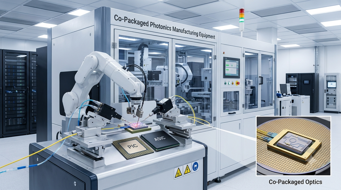
The Co-Packaged Photonics Manufacturing Equipment Market is expanding as semiconductor manufacturers invest in specialized equipment for die bonding, hybrid bonding, fiber attach, optical alignment, electro-optical testing, and 3D stacking processes. These manufacturing technologies are becoming essential for producing advanced photonic packages used in AI data centers, silicon photonics platforms, and high-performance computing systems. The global co-packaged photonics manufacturing equipment market is estimated at USD 860 million in 2025 and is projected to reach USD 4,937 million by 2032, growing at a CAGR of 28.4% from 2026 to 2032.
Source: https://www.marketsandmarkets.com, Co-Packaged Photonics Manufacturing Equipment Market https://www.marketsandmarkets.com/Market-Reports/co-packaged-photonics-manufacturing-equipment-market-165020586.html
Understanding Co-Packaged Photonics Technology
Co-packaged photonics integrates optical communication components closer to electronic processors, enabling efficient data movement within advanced computing systems.
Traditional data center architectures rely on optical transceivers connected externally to switching and computing chips. However, increasing AI workloads require significantly higher bandwidth and lower latency, creating limitations for conventional architectures.
CPO technology addresses these challenges by integrating:
- Optical engines
- Photonic integrated circuits (PICs)
- Switching chips
- Electrical interconnects
- Advanced packaging structures
The manufacturing of these systems requires highly precise equipment capable of handling optical alignment, wafer-level processing, and complex assembly operations.
AI Data Centers Driving Co-Packaged Photonics Manufacturing Equipment Market Growth
Artificial intelligence is one of the strongest growth drivers for the Co-Packaged Photonics Manufacturing Equipment Market.
Modern AI applications such as:
- Large language models
- Generative AI platforms
- Machine learning systems
- Real-time analytics
- Autonomous computing
require massive data processing capabilities.
AI data centers depend on high-speed networking infrastructure to connect thousands of GPUs, AI accelerators, and storage systems. As bandwidth requirements increase, conventional electrical interconnect technologies face challenges related to:
- Power consumption
- Signal degradation
- Heat generation
- Data transfer limitations
Co-packaged photonics enables faster optical communication while reducing energy consumption, making it a critical technology for future AI infrastructure.
Die Bonding Equipment Supporting Advanced Photonic Packaging
Die bonding is a fundamental manufacturing process in co-packaged photonics production. It involves accurately placing semiconductor dies onto substrates or interposers with extremely high precision.
Advanced die bonding equipment enables:
- High placement accuracy
- Improved thermal management
- Reliable chip integration
- High-volume manufacturing
The increasing adoption of silicon photonics and advanced semiconductor packaging is creating demand for next-generation die bonding systems capable of handling optical and electronic components simultaneously.
Manufacturers are focusing on improving:
- Bonding speed
- Alignment accuracy
- Automation capabilities
- Process reliability
These advancements are strengthening the role of die bonding equipment in the expanding Co-Packaged Photonics Manufacturing Equipment Market.
Hybrid Bonding Technology Transforming Photonic Integration
Hybrid bonding is emerging as a key technology for advanced semiconductor and photonic packaging.
Unlike traditional bonding methods that use solder connections, hybrid bonding creates direct wafer-to-wafer or die-to-wafer connections through:
- Copper-to-copper bonding
- Dielectric bonding
- Ultra-fine interconnect structures
Advantages include:
- Higher interconnect density
- Reduced signal loss
- Improved performance
- Smaller package sizes
The adoption of hybrid bonding is increasing due to demand for:
- AI accelerators
- High-bandwidth memory (HBM)
- Silicon photonics
- Advanced computing architectures
As chip architectures become more complex, hybrid bonding equipment is expected to become a critical component of future photonic manufacturing lines.
Fiber Attach Equipment Enabling Precision Optical Connectivity
Fiber attach is one of the most challenging processes in co-packaged photonics manufacturing because optical components require extremely precise alignment.
Fiber attach equipment ensures accurate positioning between:
- Optical fibers
- Photonic integrated circuits
- Laser sources
- Optical engines
High-precision fiber attachment improves:
- Optical coupling efficiency
- Signal quality
- Manufacturing yield
Automation and machine vision technologies are increasingly integrated into fiber attach systems to achieve greater accuracy and production scalability.
Download PDF Brochure @ https://www.marketsandmarkets.com/pdfdownloadNew.asp?id=165020586
Optical Alignment Systems Improving Manufacturing Accuracy
Optical alignment is a critical step in producing reliable photonic packages.
Small alignment errors can significantly impact optical performance. Therefore, advanced optical alignment equipment uses:
- Machine vision
- Automated positioning systems
- Laser measurement technologies
- Real-time feedback systems
These technologies enable manufacturers to achieve precise optical connections while reducing production errors.
As demand for high-speed optical communication increases, optical alignment equipment will remain a major growth segment within the Co-Packaged Photonics Manufacturing Equipment Market.
Electro-Optical Test Equipment Ensuring Performance Reliability
Testing plays a vital role in ensuring the performance of co-packaged photonic systems.
Electro-optical test equipment evaluates:
- Optical signal quality
- Transmission performance
- Power efficiency
- Thermal behavior
- Device reliability
As photonic packages become more complex, manufacturers require advanced testing solutions capable of identifying defects early in production.
Automated testing systems help improve:
- Manufacturing efficiency
- Product quality
- Yield rates
3D Stacking and Advanced Packaging Opportunities
Three-dimensional stacking is another important trend shaping the future of photonic manufacturing.
3D stacking enables integration of multiple layers, including:
- Logic chips
- Memory devices
- Optical components
- Photonic circuits
Benefits include:
- Higher performance
- Reduced footprint
- Improved energy efficiency
- Increased functionality
The combination of 3D stacking with co-packaged photonics creates new possibilities for next-generation AI processors and high-performance computing systems.
Silicon Photonics Accelerating Market Adoption
Silicon photonics is a major technology enabling the expansion of co-packaged photonics.
By using semiconductor manufacturing techniques to create optical components, silicon photonics provides:
- Scalability
- Cost advantages
- High integration levels
- Improved performance
Applications include:
- AI data centers
- Optical networking
- Telecommunications
- Cloud infrastructure
The growing adoption of silicon photonics is increasing demand for specialized manufacturing equipment capable of producing advanced optical semiconductor packages.
Key Market Trends Driving Growth
Increasing AI Infrastructure Investments
Global investments in AI computing infrastructure are creating strong demand for high-bandwidth optical solutions.
Growth of High-Speed Data Transmission
Cloud providers and enterprises require faster connectivity to support increasing data volumes.
Expansion of Advanced Semiconductor Packaging
Chip manufacturers are adopting advanced packaging techniques to overcome traditional scaling limitations.
Rising Demand for Energy-Efficient Computing
Co-packaged photonics reduces power consumption compared with conventional electrical interconnect solutions.
Automation in Semiconductor Manufacturing
Advanced robotics and AI-based manufacturing systems are improving production efficiency.
Challenges in Co-Packaged Photonics Manufacturing
Despite strong growth potential, the market faces several challenges.
Complex Manufacturing Processes
Producing co-packaged photonics requires highly specialized equipment and expertise.
High Initial Investment
Advanced photonic manufacturing equipment requires significant capital investment.
Yield and Reliability Challenges
Maintaining consistent quality in optical alignment and bonding processes remains technically challenging.
Supply Chain Complexity
The ecosystem requires coordination among semiconductor, optical, packaging, and equipment manufacturers.
Future Outlook of Co-Packaged Photonics Manufacturing Equipment Market
The future of the Co-Packaged Photonics Manufacturing Equipment Market is closely linked to the evolution of AI computing, cloud infrastructure, and advanced semiconductor technologies.
Future developments are expected to focus on:
- Higher optical bandwidth
- Greater packaging integration
- Automated manufacturing processes
- Improved testing technologies
- Advanced hybrid bonding solutions
As AI workloads continue expanding, data centers will require innovative approaches to overcome communication bottlenecks. Co-packaged photonics is expected to become a foundational technology enabling next-generation computing architectures.
The Co-Packaged Photonics Manufacturing Equipment Market is entering a period of rapid expansion as AI data centers, silicon photonics, and advanced semiconductor packaging technologies reshape the computing landscape.
Equipment for die bonding, hybrid bonding, fiber attach, optical alignment, electro-optical testing, and 3D stacking will play a crucial role in enabling high-performance photonic integration.
With increasing demand for faster, more efficient, and scalable computing infrastructure, co-packaged photonics is positioned to become a critical technology for future AI-driven data centers and advanced communication networks. The continued development of precision manufacturing equipment will determine the pace of adoption and commercialization of next-generation photonic systems.
FAQs – Co-Packaged Photonics Manufacturing Equipment Market
1. What is the Co-Packaged Photonics Manufacturing Equipment Market?
The Co-Packaged Photonics Manufacturing Equipment Market refers to the market for specialized manufacturing systems used to produce co-packaged photonic devices that integrate optical components with electronic chips. These equipment solutions support processes such as die bonding, hybrid bonding, fiber attach, optical alignment, electro-optical testing, and 3D stacking for advanced semiconductor and AI data center applications.
2. What factors are driving the growth of the Co-Packaged Photonics Manufacturing Equipment Market?
The major growth drivers include rising demand for AI data centers, increasing bandwidth requirements, expansion of silicon photonics, adoption of advanced semiconductor packaging, and the need for energy-efficient high-speed communication solutions. The growing complexity of AI workloads is encouraging companies to invest in next-generation optical interconnect technologies.
3. Why is co-packaged photonics important for AI data centers?
Co-packaged photonics helps AI data centers overcome limitations associated with traditional electrical interconnects by enabling faster data transfer, lower power consumption, reduced signal loss, and improved bandwidth scalability. These benefits make CPO technology essential for supporting large-scale AI training, inference, and high-performance computing workloads.
4. Which manufacturing technologies are essential in co-packaged photonics production?
Key manufacturing technologies include:
- Die bonding for precise semiconductor and photonic component integration
- Hybrid bonding for high-density chip-to-chip connections
- Fiber attach for accurate optical coupling
- Optical alignment for maintaining signal efficiency
- Electro-optical testing for performance validation
- 3D stacking for advanced multi-layer semiconductor integration
These technologies improve reliability, manufacturing yield, and performance of photonic packages.
5. What is the future outlook for the Co-Packaged Photonics Manufacturing Equipment Market?
The future outlook is positive as AI infrastructure, cloud computing, and advanced networking continue expanding. Future developments are expected to focus on higher optical bandwidth, automated manufacturing processes, improved hybrid bonding techniques, and greater adoption of silicon photonics. As data centers demand faster and more efficient communication systems, co-packaged photonics manufacturing equipment will become increasingly important in next-generation computing architectures.