Hybrid Bonding Market Trends
The semiconductor industry is entering a new era of innovation as demand for faster computing, artificial intelligence (AI), high-bandwidth memory, and advanced electronic systems continues to accelerate. Traditional chip scaling approaches are becoming increasingly challenging due to rising manufacturing complexity, power consumption concerns, and physical limitations. As a result, semiconductor manufacturers are turning toward advanced packaging technologies, with hybrid bonding emerging as one of the most promising solutions.
The Hybrid Bonding Market is gaining significant momentum as chipmakers adopt advanced 3D integration techniques to enhance performance, reduce interconnect distances, and enable higher-density semiconductor architectures. Hybrid bonding technology is becoming a critical enabler for high-performance computing (HPC), AI accelerators, chiplets, advanced memory solutions, image sensors, and next-generation logic devices. The global hybrid bonding market is projected to reach USD 633.9 million by 2032 from USD 164.7 million in 2025, registering a CAGR of 21.2% from 2025 to 2032.
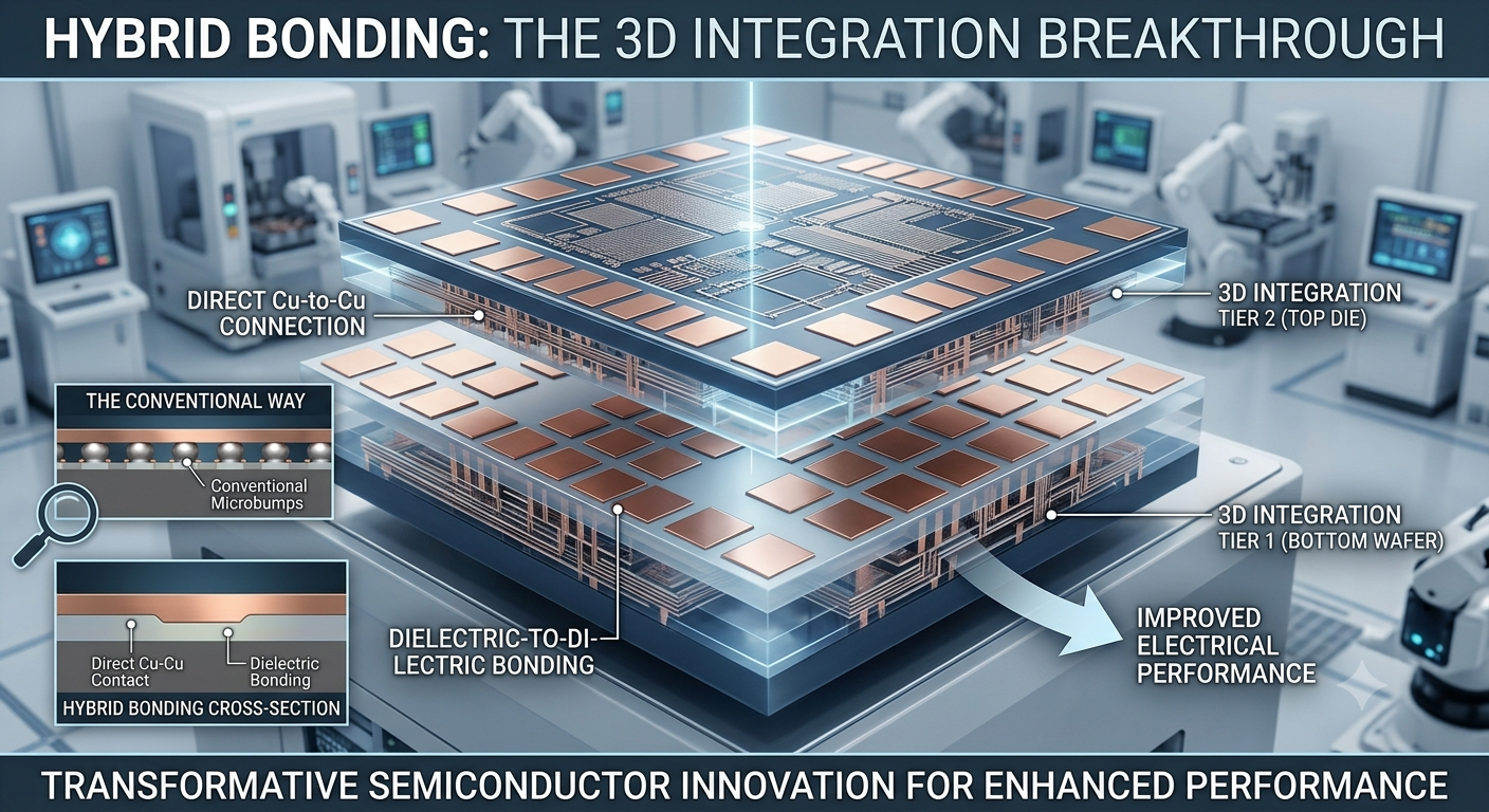
By enabling direct copper-to-copper and dielectric-to-dielectric connections without traditional solder bumps, hybrid bonding delivers superior electrical performance, improved power efficiency, and increased integration density. These advantages are positioning hybrid bonding as a key technology shaping the future of semiconductor manufacturing.
Top 10 Key Takeaways
- Hybrid bonding is transforming advanced semiconductor packaging and 3D integration.
- AI and high-performance computing are major drivers of market growth.
- Hybrid bonding improves chip performance, bandwidth, and power efficiency.
- The technology is critical for next-generation HBM memory solutions.
- Chiplet architectures are accelerating adoption of hybrid bonding.
- 3D semiconductor integration is creating new opportunities for manufacturers.
- Data centers and AI infrastructure are increasing demand for advanced packaging.
- Wafer-to-wafer and die-to-wafer bonding technologies are gaining importance.
- Asia Pacific remains a key region for semiconductor manufacturing growth.
- Hybrid bonding will be essential for future AI processors and advanced computing systems.
Understanding Hybrid Bonding Technology
Hybrid bonding is an advanced semiconductor packaging technology that creates direct connections between two semiconductor surfaces through a combination of dielectric bonding and metal interconnect bonding.
Unlike conventional bonding techniques that rely on solder bumps or adhesives, hybrid bonding enables:
- Direct copper-to-copper connections
- Ultra-fine pitch interconnects
- Lower electrical resistance
- Higher bandwidth communication
- Improved thermal performance
- Greater chip density
The technology is widely used in applications requiring extreme performance and miniaturization, including AI processors, memory stacks, and advanced computing systems.
Download PDF Brochure @ https://www.marketsandmarkets.com/pdfdownloadNew.asp?id=2641237
AI and High-Performance Computing Driving Market Growth
The rapid expansion of artificial intelligence and high-performance computing is one of the strongest drivers of the Hybrid Bonding Market.
Modern AI workloads require enormous computational power and memory bandwidth for:
- Large language model training
- Generative AI applications
- Machine learning algorithms
- Data analytics
- Scientific simulations
Hybrid bonding enables closer integration between processing units and memory components, reducing latency and improving data transfer speeds.
AI accelerators increasingly depend on advanced packaging solutions that combine:
- Logic chips
- High-bandwidth memory (HBM)
- Chiplets
- Specialized AI processors
Hybrid bonding provides the foundation for these high-density architectures, making it essential for future AI infrastructure.
Growing Adoption in High-Bandwidth Memory (HBM)
High-bandwidth memory has become a critical component in AI servers, GPUs, and HPC systems. As AI models become larger and more complex, the demand for faster memory access continues to increase.
Hybrid bonding improves HBM performance by enabling:
- More memory stack layers
- Smaller interconnect distances
- Higher bandwidth
- Lower power consumption
Advanced memory manufacturers are increasingly exploring hybrid bonding technologies to support future generations of HBM solutions.
The combination of hybrid bonding and HBM is expected to play a major role in next-generation AI computing platforms.
Chiplet Architecture Accelerating Hybrid Bonding Adoption
The rise of chiplet-based designs is creating new opportunities for hybrid bonding technology.
Chiplets allow semiconductor manufacturers to combine multiple smaller dies into a single package rather than creating a large monolithic chip.
Hybrid bonding enables efficient communication between chiplets by providing:
- High-density interconnects
- Reduced signal loss
- Faster data transfer
- Improved scalability
As companies increasingly adopt heterogeneous integration strategies, hybrid bonding is becoming a key technology for connecting advanced chip components.
3D Semiconductor Integration Transforming Chip Design
Three-dimensional integrated circuits (3D ICs) are becoming increasingly important as semiconductor companies seek higher performance within smaller form factors.
Hybrid bonding supports advanced 3D integration by allowing:
- Vertical chip stacking
- Increased transistor density
- Better power efficiency
- Shorter communication pathways
Applications benefiting from 3D hybrid bonding include:
- AI processors
- Memory devices
- Image sensors
- Logic circuits
- Advanced processors
The transition toward 3D semiconductor architectures is expected to significantly accelerate hybrid bonding adoption.
Advanced Packaging Becoming a Strategic Priority
As traditional transistor scaling slows, advanced packaging has become a major focus area for semiconductor innovation.
Hybrid bonding offers several advantages compared with traditional packaging methods:
Improved Performance
Shorter interconnect paths enable faster signal transmission and improved processing capabilities.
Reduced Power Consumption
Lower electrical resistance helps minimize energy usage.
Higher Integration Density
Manufacturers can integrate more functionality into smaller packages.
Enhanced Scalability
Hybrid bonding supports future semiconductor architectures beyond conventional scaling.
These benefits make hybrid bonding a strategic technology for semiconductor manufacturers worldwide.
Applications Expanding Across Multiple Industries
Data Centers and Cloud Computing
The growth of cloud computing and AI-powered data centers is increasing demand for advanced processors and memory solutions.
Hybrid bonding supports:
- AI servers
- High-performance processors
- Accelerated computing systems
- Advanced networking hardware
As data centers require greater efficiency and computing power, hybrid bonding adoption is expected to increase.
Consumer Electronics
Smartphones, wearables, and advanced electronics require compact and powerful semiconductor solutions.
Hybrid bonding enables:
- Smaller chip packages
- Improved processing performance
- Enhanced camera technologies
- Better energy efficiency
Image sensors, particularly advanced CMOS sensors, are among the important applications benefiting from hybrid bonding.
Automotive Electronics
The automotive industry is rapidly adopting advanced semiconductor technologies for:
- Autonomous driving
- Advanced driver assistance systems (ADAS)
- Electric vehicles
- Vehicle computing platforms
Hybrid bonding enables automotive chips to deliver higher processing capability while maintaining compact designs.
Healthcare and Imaging Systems
Medical imaging devices require high-resolution sensors and advanced processing capabilities.
Hybrid bonding supports:
- CMOS image sensors
- High-performance imaging systems
- Diagnostic equipment
- Scientific instruments
The growing demand for precision imaging technologies is creating additional market opportunities.
Key Technology Trends Shaping the Hybrid Bonding Market
Increasing Wafer-to-Wafer Bonding Adoption
Wafer-to-wafer hybrid bonding is gaining traction for applications requiring high-volume production and excellent alignment accuracy.
Expansion of Die-to-Wafer Bonding
Die-to-wafer bonding provides greater flexibility for heterogeneous integration by allowing different chip components to be combined.
Smaller Interconnect Pitch
Continuous advancements are enabling finer bonding pitches, improving performance and integration density.
Integration with Chiplet Ecosystems
Hybrid bonding is becoming increasingly important for advanced chiplet architectures and modular semiconductor designs.
Improved Manufacturing Automation
Automation and precision alignment technologies are improving production efficiency and reducing manufacturing challenges.
Challenges Affecting Market Growth
Despite strong growth opportunities, the Hybrid Bonding Market faces several challenges.
High Manufacturing Complexity
Hybrid bonding requires extremely precise surface preparation, alignment, and contamination control.
Expensive Equipment Requirements
Advanced bonding equipment and semiconductor fabrication infrastructure require significant investment.
Yield Management Issues
Maintaining high production yields remains a challenge as bonding processes become more complex.
Limited Standardization
The semiconductor industry continues developing standards for advanced packaging and hybrid bonding processes.
Addressing these challenges will be essential for wider adoption.
Regional Market Outlook
North America
North America is a major hub for semiconductor innovation, AI development, and advanced computing. Strong investments in AI infrastructure and semiconductor research are supporting hybrid bonding adoption.
Asia Pacific
Asia Pacific is expected to remain a dominant region due to its strong semiconductor manufacturing ecosystem. Countries such as Taiwan, South Korea, Japan, and China are investing heavily in advanced packaging technologies.
Europe
Europe is increasing investments in semiconductor manufacturing, automotive electronics, and research initiatives focused on advanced chip technologies.
Future Outlook of the Hybrid Bonding Market
The future of the Hybrid Bonding Market will be strongly influenced by AI expansion, advanced computing requirements, and the evolution of semiconductor packaging.
Future developments are expected to include:
- AI-specific 3D chip architectures
- Next-generation HBM solutions
- Advanced chiplet integration
- Smaller bonding pitches
- Higher-density semiconductor packages
- Improved automation technologies
- Integration with emerging computing platforms
As semiconductor designers continue searching for alternatives to traditional scaling methods, hybrid bonding will become increasingly important in enabling powerful, efficient, and compact electronic systems.
The Hybrid Bonding Market is becoming a cornerstone technology for the future of semiconductor innovation. Driven by the rapid growth of AI, high-performance computing, advanced memory solutions, and chiplet architectures, hybrid bonding is enabling unprecedented levels of integration and performance.
Although challenges related to cost, manufacturing complexity, and process optimization remain, ongoing advancements in semiconductor packaging are accelerating adoption. As the demand for faster, smaller, and more energy-efficient computing systems continues to rise, hybrid bonding will play a critical role in shaping the next generation of AI chips, HPC platforms, and advanced electronic devices.
Frequently Asked Questions (FAQs)
1. What is hybrid bonding technology?
Hybrid bonding is an advanced semiconductor packaging method that directly connects semiconductor dies using copper-to-copper and dielectric bonding, enabling high-density chip integration.
2. Why is hybrid bonding important for AI chips?
Hybrid bonding improves data transfer speed, reduces latency, and enables integration of processors with high-bandwidth memory, making it ideal for AI workloads.
3. What applications use hybrid bonding?
Hybrid bonding is used in AI processors, high-performance computing systems, HBM memory, CMOS image sensors, chiplets, consumer electronics, and automotive semiconductor applications.
4. What are the advantages of hybrid bonding compared with traditional packaging?
Hybrid bonding provides higher bandwidth, lower power consumption, smaller interconnects, improved thermal performance, and greater integration density.
5. What is the future outlook for the Hybrid Bonding Market?
The market is expected to grow significantly as semiconductor manufacturers adopt advanced packaging technologies to support AI, cloud computing, chiplets, and next-generation computing platforms.
About MarketsandMarkets™
MarketsandMarkets™ has been recognized as one of America’s Best Management Consulting Firms by Forbes, as per their recent report.
MarketsandMarkets™ is a blue ocean alternative in growth consulting and program management, leveraging a man-machine offering to drive supernormal growth for progressive organizations in the B2B space. With the widest lens on emerging technologies, we are proficient in co-creating supernormal growth for clients across the globe.
Today, 80% of Fortune 2000 companies rely on MarketsandMarkets, and 90 of the top 100 companies in each sector trust us to accelerate their revenue growth. With a global clientele of over 13,000 organizations, we help businesses thrive in a disruptive ecosystem.
The B2B economy is witnessing the emergence of $25 trillion in new revenue streams that are replacing existing ones within this decade. We work with clients on growth programs, helping them monetize this $25 trillion opportunity through our service lines – TAM Expansion, Go-to-Market (GTM) Strategy to Execution, Market Share Gain, Account Enablement, and Thought Leadership Marketing.
Built on the ‘GIVE Growth’ principle, we collaborate with several Forbes Global 2000 B2B companies to keep them future-ready. Our insights and strategies are powered by industry experts, cutting-edge AI, and our Market Intelligence Cloud, KnowledgeStore™, which integrates research and provides ecosystem-wide visibility into revenue shifts.
To find out more, visit www.MarketsandMarkets™.com or follow us on Twitter , LinkedIn and Facebook .
Contact:
Mr. Rohan Salgarkar
MarketsandMarkets™ INC.
1615 South Congress Ave.
Suite 103, Delray Beach, FL 33445
USA: +1-888-600-6441
