The semiconductor industry is undergoing a major transformation as demand for artificial intelligence (AI), high-performance computing (HPC), advanced memory, and next-generation electronic devices continues to increase. Traditional semiconductor packaging technologies are facing limitations in delivering the higher bandwidth, lower latency, improved energy efficiency, and greater integration density required by modern computing applications. Against this backdrop, hybrid bonding is emerging as a critical technology for next-generation semiconductor manufacturing.
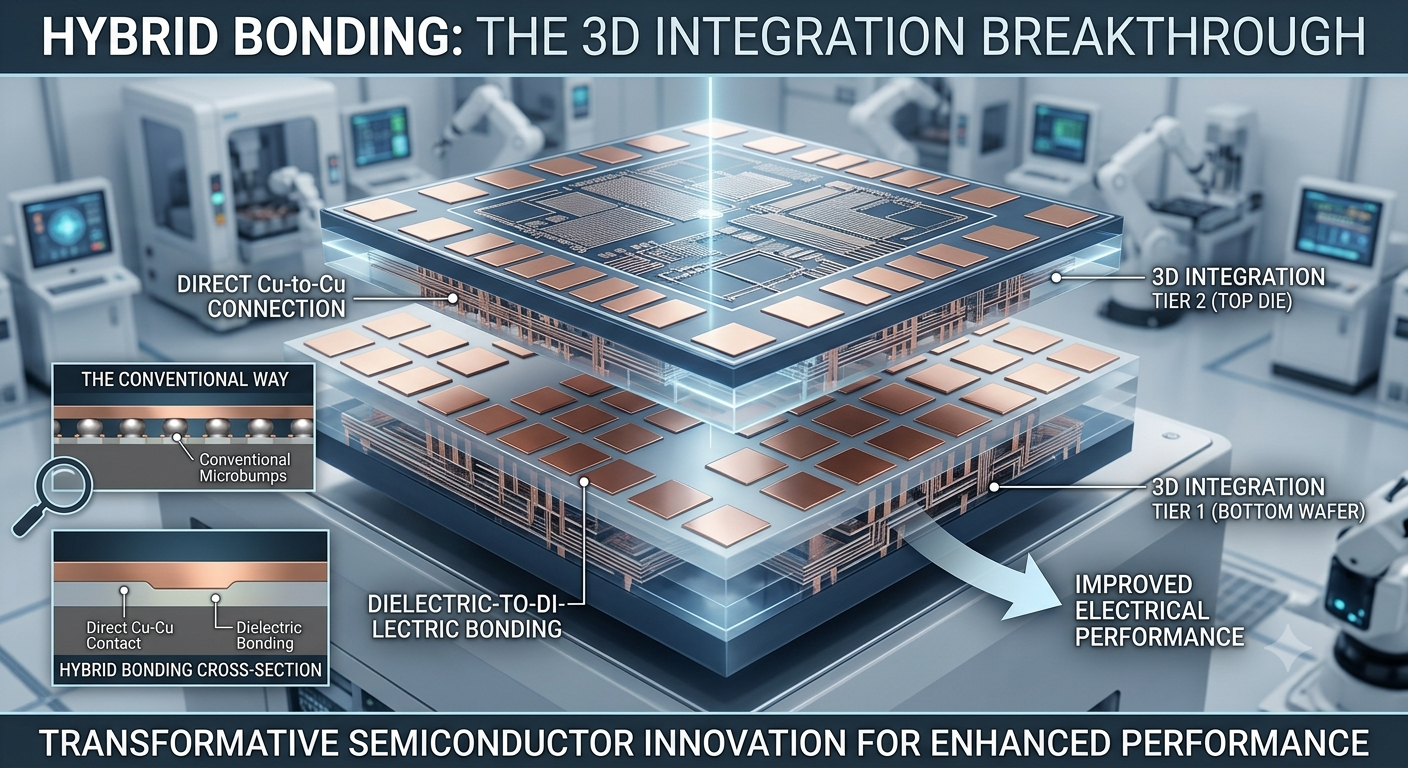
The Hybrid Bonding Market Analysis highlights the growing importance of advanced packaging solutions in enabling high-density interconnections between semiconductor dies and wafers. Hybrid bonding combines dielectric-to-dielectric bonding with direct metal-to-metal connections, particularly copper-to-copper bonding, to create highly integrated semiconductor structures. This approach reduces interconnect distances and supports improved electrical performance compared with conventional micro-bump-based packaging techniques.
According to MarketsandMarkets, The hybrid bonding market is projected to be valued at USD 0.38 billion in 2026 and USD 2.45 billion by 2033, exhibiting a CAGR of 30.3% during the forecast period. Increasing investments in AI processors, high-bandwidth memory (HBM), chiplet architectures, and 3D integrated circuits are expected to create significant growth opportunities.
As semiconductor manufacturers focus on improving chip performance while reducing power consumption and physical size, hybrid bonding is becoming an important technology for the future of advanced packaging.
Growing Demand for High-Performance Computing
High-performance computing is one of the major factors supporting the expansion of the hybrid bonding market. Applications such as generative AI, machine learning, scientific simulations, cloud computing, and data analytics require semiconductor processors capable of handling increasingly complex workloads.
Traditional packaging approaches often face limitations in supporting the growing communication requirements between processors and memory components. Hybrid bonding addresses these limitations by enabling extremely fine-pitch interconnections and shorter electrical pathways between semiconductor dies.
The technology allows manufacturers to integrate multiple dies vertically, improving communication speeds and reducing signal transmission distances. These capabilities are particularly important for AI accelerators, graphics processing units (GPUs), and advanced computing processors.
The increasing deployment of AI infrastructure and hyperscale data centers is also creating demand for semiconductor devices that deliver higher computational performance with improved energy efficiency. Consequently, the Hybrid Bonding Market Analysis identifies high-performance computing as an important application area for future technology adoption.
Download PDF Brochure @ https://www.marketsandmarkets.com/pdfdownloadNew.asp?id=2641237
Increasing Adoption of 3D Semiconductor Integration
Three-dimensional semiconductor integration is transforming the way manufacturers design and produce advanced chips. Instead of relying entirely on traditional two-dimensional layouts, semiconductor companies are increasingly stacking multiple dies vertically to improve functionality and reduce package size.
Hybrid bonding supports this transition by enabling direct connections between stacked semiconductor components. Its ability to create high-density interconnections makes it suitable for advanced logic devices, memory components, image sensors, and heterogeneous integration applications.
The technology supports different packaging architectures, including wafer-to-wafer (W2W), die-to-wafer (D2W), and die-to-die (D2D) bonding.
Wafer-to-wafer bonding enables the connection of two complete wafers, making it suitable for applications requiring uniform integration across multiple semiconductor layers. Die-to-wafer bonding allows individual dies to be attached to a target wafer, providing greater flexibility when integrating different semiconductor components. Die-to-die bonding supports direct integration between individual chips.
Among these architectures, die-to-wafer bonding is expected to experience significant growth. MarketsandMarkets projects this segment to register a CAGR of 44.2% during the forecast period, supported by growing demand for chiplets, HBM, AI accelerators, and advanced computing applications.
High-Bandwidth Memory Creates New Growth Opportunities
High-bandwidth memory is becoming increasingly important as AI and HPC applications require faster access to large volumes of data. Modern AI processors depend on advanced memory architectures to support parallel computing, large language models, and complex machine learning operations.
Hybrid bonding offers opportunities to improve memory integration by enabling dense vertical connections between memory dies and logic components. Compared with conventional interconnect approaches, the technology supports smaller connection pitches and potentially higher interconnect density.
The growing adoption of 3D-stacked memory is encouraging semiconductor manufacturers to explore advanced bonding processes. Hybrid bonding can support the development of next-generation memory devices by improving connectivity between stacked layers and reducing the physical distance through which data must travel.
As AI infrastructure expands, the demand for efficient memory bandwidth is expected to increase. This creates opportunities for equipment manufacturers, semiconductor foundries, materials suppliers, and advanced packaging providers operating across the Hybrid Bonding Market.
Key Technology Trends Shaping the Hybrid Bonding Market
Several technological developments are influencing the evolution of the industry.
Copper-to-Copper Bonding: Copper-to-copper bonding is gaining importance because it enables direct electrical connections between semiconductor components. It supports fine-pitch interconnects and higher connection density, making it suitable for advanced 3D integration and high-performance processors.
Heterogeneous Integration: Semiconductor manufacturers are increasingly integrating different types of chips within a single package. Hybrid bonding enables the combination of logic, memory, sensing, and communication components, supporting more compact and efficient semiconductor architectures.
Advanced Surface Preparation: Surface cleanliness and precision are essential for successful hybrid bonding. Improvements in cleaning, plasma activation, planarization, and contamination control are helping manufacturers achieve reliable bonding and improve production yields.
Precision Alignment and Metrology: Advanced alignment and inspection technologies are becoming essential as semiconductor interconnect pitches continue to shrink. Improved metrology solutions help manufacturers identify defects, maintain bonding accuracy, and increase process consistency.
Back-End Semiconductor Processing: Back-end hybrid bonding is gaining importance as manufacturers expand investments in advanced packaging. Processes such as wafer thinning, dicing, surface cleaning, alignment, bonding, and annealing play an important role in achieving reliable semiconductor integration.
AI and Data Centers Accelerate Market Expansion
The rapid development of AI technologies is creating new requirements for semiconductor performance. AI training and inference workloads involve extensive data movement between processors, memory, and other computing components. Conventional packaging methods may struggle to deliver the required bandwidth and energy efficiency at increasingly advanced integration levels.
Hybrid bonding provides a pathway toward developing highly integrated semiconductor architectures that support faster communication between processing and memory components. This makes the technology particularly relevant for AI accelerators, advanced GPUs, and next-generation data center processors.
Data center operators are also prioritizing energy-efficient computing infrastructure to manage increasing electricity consumption and operational costs. Semiconductor technologies that improve performance per watt are therefore becoming strategically important.
The Hybrid Bonding Market Analysis indicates that the increasing need for ultra-dense logic-to-memory connectivity in AI and machine learning accelerators will create attractive opportunities for technology providers. As computing workloads become more demanding, hybrid bonding is expected to play a greater role in supporting advanced semiconductor packaging.
Automotive and Consumer Electronics Applications
Although high-performance computing is an important growth area, hybrid bonding is also finding opportunities across automotive and consumer electronics applications.
In the automotive industry, the growing integration of advanced driver-assistance systems (ADAS), autonomous driving technologies, in-vehicle computing, and high-resolution imaging systems is increasing demand for advanced semiconductor devices.
Hybrid bonding can support compact chip integration and high-density interconnections required by advanced automotive electronics. The technology is also relevant to CMOS image sensors used in automotive cameras and imaging applications.
Consumer electronics manufacturers are continuously working to develop smaller, lighter, and more powerful electronic devices. Hybrid bonding can support compact semiconductor packaging and improved performance in image sensors, advanced processors, and other electronic components.
The increasing use of augmented reality (AR), virtual reality (VR), and wearable technologies may also create opportunities for hybrid bonding in advanced sensing and imaging applications.
Asia Pacific Leads Semiconductor Manufacturing Growth
Asia Pacific represents an important regional market for hybrid bonding due to its strong semiconductor manufacturing ecosystem and increasing investments in advanced packaging technologies.
According to MarketsandMarkets, Asia Pacific accounted for approximately 52.3% of the global hybrid bonding market share in 2025. Countries such as Taiwan, South Korea, Japan, and China are supporting regional growth through investments in semiconductor fabrication, memory manufacturing, foundries, and advanced packaging infrastructure.
Taiwan plays an important role in advanced semiconductor manufacturing and heterogeneous integration. South Korea has a strong presence in memory manufacturing, while Japan contributes through semiconductor equipment, materials, and manufacturing technologies. China’s expanding semiconductor ecosystem is also supporting demand for advanced packaging solutions.
The region’s established semiconductor supply chain and growing investments in AI processors, HBM, and 3D integrated circuits are expected to strengthen its position in the global Hybrid Bonding Market.
Competitive Landscape and Key Market Players
The competitive landscape includes semiconductor equipment manufacturers, advanced packaging technology providers, materials suppliers, and semiconductor process developers. Companies are focusing on improving bonding accuracy, production throughput, surface preparation, and manufacturing yield.
Key players identified by MarketsandMarkets include:
- BE Semiconductor Industries (Besi)
- Tokyo Electron Limited
- EV Group (EVG)
- Piotech, Inc.
- ASMPT
- Applied Materials, Inc.
- SUSS MicroTec SE
- Kulicke & Soffa Industries, Inc.
- Shibaura Mechatronics Corporation
- Bondtech Co., Ltd.
These companies are investing in advanced bonding equipment, process technologies, and integrated manufacturing solutions to address the requirements of next-generation semiconductor applications.
Strategic collaborations are also supporting technology development. Equipment manufacturers and semiconductor process companies are working together to improve wafer bonding, die placement, metrology, and surface preparation capabilities. Such partnerships can help accelerate the commercialization of hybrid bonding and support its transition into high-volume semiconductor manufacturing.
Challenges Affecting Market Adoption
Despite its strong growth potential, the hybrid bonding industry faces several challenges.
One of the major restraints is the substantial capital investment required to establish advanced bonding manufacturing facilities. Hybrid bonding requires specialized equipment for wafer bonding, cleaning, alignment, surface preparation, and metrology. These investments can create barriers for smaller semiconductor manufacturers and new market participants.
Maintaining extremely clean and defect-free surfaces is another important challenge. Even small particles or surface irregularities can affect bonding quality and manufacturing yield. As interconnect pitches become smaller, maintaining consistent surface conditions and accurate alignment becomes increasingly difficult.
The industry also faces challenges associated with standardization across die formats, pad structures, and surface preparation processes. Developing scalable manufacturing processes that deliver consistent performance across different semiconductor architectures will be important for wider adoption.
Continuous improvements in process control, inspection systems, and equipment capabilities are expected to address these challenges over time.
Future Outlook: Hybrid Bonding Creates New Semiconductor Opportunities
The future of the hybrid bonding industry will be closely connected to advancements in AI computing, 3D semiconductor integration, HBM, chiplet architectures, and advanced packaging technologies.
As semiconductor manufacturers seek to overcome the limitations of traditional packaging, hybrid bonding is expected to become increasingly important for enabling high-density interconnections and improved chip performance.
The projected growth from USD 0.38 billion in 2026 to USD 2.45 billion by 2033 reflects the increasing commercial importance of this technology. Strong demand for AI accelerators, advanced memory, and energy-efficient computing solutions is expected to support market expansion.
The Hybrid Bonding Market Analysis highlights significant opportunities for semiconductor equipment manufacturers, foundries, materials suppliers, and technology developers. Companies that focus on precision bonding, advanced metrology, contamination control, and scalable manufacturing processes will be well positioned to benefit from the industry’s evolution.
Overall, hybrid bonding is moving beyond a specialized semiconductor manufacturing process and becoming an important enabler of next-generation computing. Its role in improving connectivity, integration density, and energy efficiency is expected to shape the future of advanced semiconductor packaging.
FAQs
Q1. What is the projected size of the hybrid bonding market?
The hybrid bonding market is projected to grow from USD 0.38 billion in 2026 to USD 2.45 billion by 2033, registering a CAGR of 30.3% during the forecast period.
Q2. What are the key factors driving the growth of the hybrid bonding market?
Increasing demand for high-performance computing, artificial intelligence (AI), high-bandwidth memory (HBM), 3D semiconductor integration, and advanced packaging technologies is driving market growth.
Q3. Which bonding technology is widely used in the hybrid bonding market?
Copper-to-copper bonding combined with dielectric-to-dielectric bonding is a key technology, enabling high-density interconnections and improved semiconductor performance.
Q4. Which region dominates the hybrid bonding market?
Asia Pacific dominates the hybrid bonding market, supported by strong semiconductor manufacturing capabilities and investments in advanced packaging across Taiwan, South Korea, Japan, and China.
Q5. Who are the key players in the hybrid bonding market?
Major players include BE Semiconductor Industries (Besi), Tokyo Electron, EV Group, ASMPT, Applied Materials, SUSS MicroTec, Kulicke & Soffa Industries, Piotech, Shibaura Mechatronics, and Bondtech.
About MarketsandMarkets™
MarketsandMarkets™ has been recognized as one of America’s Best Management Consulting Firms by Forbes, as per their recent report.
MarketsandMarkets™ is a blue ocean alternative in growth consulting and program management, leveraging a man-machine offering to drive supernormal growth for progressive organizations in the B2B space. With the widest lens on emerging technologies, we are proficient in co-creating supernormal growth for clients across the globe.
Today, 80% of Fortune 2000 companies rely on MarketsandMarkets, and 90 of the top 100 companies in each sector trust us to accelerate their revenue growth. With a global clientele of over 13,000 organizations, we help businesses thrive in a disruptive ecosystem.
The B2B economy is witnessing the emergence of $25 trillion in new revenue streams that are replacing existing ones within this decade. We work with clients on growth programs, helping them monetize this $25 trillion opportunity through our service lines – TAM Expansion, Go-to-Market (GTM) Strategy to Execution, Market Share Gain, Account Enablement, and Thought Leadership Marketing.
Built on the ‘GIVE Growth’ principle, we collaborate with several Forbes Global 2000 B2B companies to keep them future-ready. Our insights and strategies are powered by industry experts, cutting-edge AI, and our Market Intelligence Cloud, KnowledgeStore™, which integrates research and provides ecosystem-wide visibility into revenue shifts.
To find out more, visit www.MarketsandMarkets™.com or follow us on Twitter , LinkedIn and Facebook .
Contact:
Mr. Rohan Salgarkar
MarketsandMarkets™ INC.
1615 South Congress Ave.
Suite 103, Delray Beach, FL 33445
USA: +1-888-600-6441