The semiconductor industry is undergoing a major transformation as demand for high-performance computing, artificial intelligence (AI), cloud computing, and advanced digital infrastructure continues to increase. Traditional monolithic chip designs are becoming more challenging to scale because of rising manufacturing costs, design complexity, power consumption, and physical limitations. In this environment, chiplet technology is emerging as an important solution for developing powerful, scalable, and energy-efficient semiconductor systems. The Chiplet Market Growth trajectory reflects the growing adoption of modular chip architectures across data centers, AI computing platforms, and high-performance computing (HPC) applications.
Chiplets are smaller, specialized semiconductor dies that are integrated into a single package to perform different computing functions. Instead of manufacturing an entire processor on one large silicon die, semiconductor companies can combine multiple chiplets designed for processing, memory, input/output (I/O), and AI acceleration. This modular approach enables manufacturers to optimize individual components, improve production flexibility, and develop advanced processors more efficiently.
According to MarketsandMarkets, the global chiplet market was valued at USD 51.94 billion in 2025 and is projected to reach USD 157.23 billion by 2030, registering a compound annual growth rate (CAGR) of 24.8% during the forecast period. Increasing investments in data center infrastructure, AI accelerators, advanced packaging, and heterogeneous integration are expected to support this expansion. As organizations demand greater computing capabilities, chiplet technology is becoming an important foundation for next-generation semiconductor innovation.
Data Center Expansion Creates New Chiplet Market Growth Opportunities
The rapid expansion of cloud computing and hyperscale data centers is creating significant opportunities for chiplet manufacturers. Enterprises increasingly rely on cloud-based applications, large-scale databases, real-time analytics, and digital platforms to manage business operations. These workloads require processors that can deliver high computational throughput while maintaining energy efficiency and operational reliability.
Chiplet-based architectures allow semiconductor manufacturers to combine processing cores, memory interfaces, networking components, and specialized accelerators within a single package. This integration can improve data movement, support scalable processor configurations, and enable manufacturers to tailor chip designs to specific workloads.
Hyperscale data centers represent a particularly important opportunity. Cloud service providers are investing in infrastructure to support generative AI, machine learning, high-volume transactions, and enterprise software. These applications place increasing demands on processors and accelerators, encouraging semiconductor companies to develop customized chiplet-based solutions.
The Chiplet Market Growth opportunity also extends to networking and storage infrastructure. Data centers require high-speed interconnects, efficient data processing, and low-latency communication between computing components. Chiplet integration can help manufacturers develop processors that combine specialized functions while reducing the need to design every component as part of a single monolithic die.
In addition, chiplet architectures offer opportunities to improve manufacturing economics. Smaller dies can provide better manufacturing yields than comparably complex large dies under suitable design and process conditions. Manufacturers can also reuse established chiplets across multiple products, potentially reducing development time and engineering expenses. However, these benefits depend on packaging costs, integration complexity, testing requirements, and the design of the overall system.
Artificial Intelligence Accelerates Chiplet Market Growth
Artificial intelligence is emerging as one of the most important drivers of the chiplet industry. Generative AI, deep learning, natural language processing, and computer vision require substantial computing power and high-speed data transfer. Conventional processors may struggle to meet the performance and efficiency requirements of increasingly complex AI workloads, encouraging the adoption of specialized computing architectures.
Chiplet technology enables semiconductor companies to combine CPUs, GPUs, AI accelerators, memory interfaces, and other functional components within a single package. This flexibility supports the development of processors optimized for model training, inference, and data-intensive computing applications.
AI ASIC coprocessors represent a promising area of opportunity because they are designed to execute specific computational workloads efficiently. According to MarketsandMarkets, the AI ASIC coprocessor segment is projected to experience the fastest growth among processor categories during the forecast period. Rising demand for AI infrastructure, customized accelerators, and energy-efficient computing systems is expected to support this trend.
Another important factor influencing Chiplet Market Growth is the need to improve performance per watt. AI data centers consume substantial amounts of electricity, particularly when operating large GPU clusters and high-density accelerator systems. Chiplet architectures can support more efficient system designs by enabling specialized components to be integrated according to workload requirements. Nevertheless, the overall energy savings depend on interconnect efficiency, packaging design, cooling, and system-level implementation.
The expansion of AI computing also creates opportunities for semiconductor design companies, advanced packaging providers, testing specialists, and intellectual property vendors. Businesses that can deliver reliable chiplet integration, high-bandwidth connectivity, and scalable manufacturing solutions are positioned to benefit from growing AI infrastructure investments.
Download PDF Brochure @ https://www.marketsandmarkets.com/pdfdownloadNew.asp?id=131809383
High-Performance Computing Strengthens Market Demand
High-performance computing is another major application area supporting Chiplet Market Growth. HPC systems are widely used in scientific research, weather forecasting, financial modeling, engineering simulations, healthcare research, and industrial design. These applications require processors capable of handling large datasets, complex calculations, and parallel workloads.
Chiplet architectures allow manufacturers to scale computing performance by combining multiple processing dies and specialized components within a package. This approach is particularly useful when developing processors that exceed the practical manufacturing or design limits of a single large die.
In scientific computing, chiplet-based processors can support simulations involving climate models, molecular structures, fluid dynamics, and complex physical systems. In financial services, advanced computing platforms can accelerate risk analysis, quantitative modeling, and large-scale data processing. Manufacturing organizations can also use HPC systems to support digital twins, computational engineering, and product optimization.
The demand for faster data movement is equally important. HPC workloads often require processors to exchange large volumes of information with memory and other processing units. Advanced packaging technologies, including two-dimensional arrangements using high-density interconnects and three-dimensional chip stacking, can help improve connectivity between chiplets.
As HPC infrastructure evolves toward larger and more specialized computing systems, semiconductor manufacturers are expected to explore chiplet designs that balance computational performance, bandwidth, power consumption, and manufacturing cost. These requirements create opportunities for chiplet developers, packaging companies, and providers of high-speed interconnect technologies.
Advanced Packaging Technologies Drive Innovation
Advanced packaging is a critical enabler of Chiplet Market Growth because it determines how effectively separate semiconductor dies communicate and operate as one integrated system. As conventional transistor scaling becomes increasingly complex and expensive, semiconductor companies are investing in packaging technologies that improve performance without relying exclusively on smaller process nodes.
Among the available approaches, 2.5D and 3D packaging are gaining importance. In 2.5D packaging, multiple dies are placed side by side and connected through a high-density interposer. In 3D packaging, semiconductor dies are stacked vertically to reduce interconnect distances and support compact designs.
These technologies are particularly valuable for AI accelerators, HPC processors, and advanced server platforms. They enable close integration between computing dies and high-bandwidth memory, helping systems transfer large volumes of data efficiently. Improvements in interconnect density can also reduce communication delays and improve overall system performance.
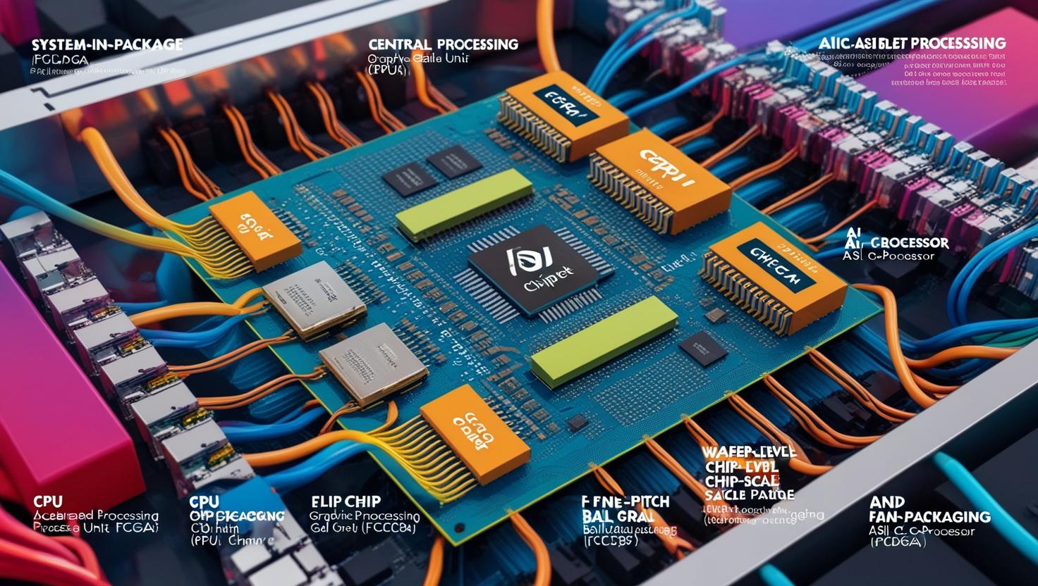
Other packaging technologies, including system-in-package (SiP), flip-chip ball grid array (FCBGA), flip-chip chip-scale package (FCCSP), wafer-level chip-scale packaging (WLCSP), and fan-out packaging, serve different product requirements. The choice depends on performance targets, package dimensions, thermal conditions, production volumes, and cost considerations.
The expansion of advanced packaging creates business opportunities for semiconductor foundries, outsourced semiconductor assembly and test providers, equipment manufacturers, and materials suppliers. Companies that improve packaging yield, manufacturing throughput, and thermal performance can strengthen their position in the evolving chiplet ecosystem.
Heterogeneous Integration and Open Standards Create Opportunities
Heterogeneous integration is a fundamental principle behind chiplet-based semiconductor design. It enables different types of semiconductor dies to work together in one package, even when they use different manufacturing processes or serve different functions.
For example, a processor package may combine advanced compute dies with I/O dies, memory interfaces, analog components, and specialized accelerators. This architecture allows manufacturers to select suitable technologies for individual functions rather than manufacturing every component using the same process node.
This flexibility creates opportunities to reuse proven designs, develop product variants, and accelerate innovation. Semiconductor companies can potentially introduce processors for different performance and price categories by changing the number or configuration of chiplets.
However, integration across suppliers requires reliable communication interfaces. The Universal Chiplet Interconnect Express (UCIe) standard is an important industry initiative designed to support communication between chiplets. Wider adoption of interoperable interfaces could enable a more flexible ecosystem in which companies source compatible components from different vendors.
For the Chiplet Market Growth outlook, standardization can expand opportunities beyond large integrated semiconductor manufacturers. Specialized designers may develop chiplets for memory connectivity, security, acceleration, or networking, while packaging providers integrate these components into complete systems.
Nevertheless, interoperability requires more than a common interface. Compatibility across power delivery, thermal design, testing, reliability, and software must also be addressed. Progress in these areas will influence how quickly multi-vendor chiplet ecosystems become commercially viable.
Regional Outlook: Asia Pacific and North America
Regional semiconductor manufacturing capabilities, research investments, and demand for advanced computing are shaping the global chiplet industry.
Asia Pacific is positioned as a major growth center because of its semiconductor foundries, packaging infrastructure, electronics manufacturing base, and investments in AI and 5G technologies. Taiwan, South Korea, China, and Japan play important roles in semiconductor production, memory technologies, materials, and advanced packaging. India is also expanding its semiconductor ambitions, creating potential opportunities for design services, manufacturing partnerships, and supporting infrastructure.
MarketsandMarkets identifies Asia Pacific as a key regional market, supported by its manufacturing ecosystem and rising demand for advanced computing. Its regional analysis projects a CAGR of 25.9% for the Asia Pacific chiplet market during 2025–2030. This expansion could create opportunities for packaging suppliers, semiconductor designers, equipment manufacturers, and technology companies serving data center and AI applications.
North America also represents an important market because of its concentration of semiconductor designers, hyperscale cloud providers, AI developers, and research organizations. Investments in domestic semiconductor capabilities and advanced computing infrastructure can encourage demand for chiplet-based processors and specialized accelerators.
Europe offers additional opportunities through semiconductor research, industrial computing, automotive electronics, and collaborative development programs. Across these regions, supply chain resilience, access to advanced packaging capacity, and cooperation between chip designers and manufacturing partners will remain important competitive factors.
Challenges Affecting Chiplet Market Growth
Despite its strong growth potential, the chiplet industry faces technical and commercial challenges. One of the most important is thermal management. Combining multiple high-performance dies in a compact package can create concentrated heat, particularly in AI accelerators and HPC processors. Manufacturers must develop effective cooling systems, thermal interfaces, and package designs to maintain reliable operation.
Advanced packaging also involves significant investment in equipment, materials, process development, and testing. Although chiplets can reduce some manufacturing costs, the additional packaging and integration steps may offset those benefits in certain applications. Companies must evaluate the total cost of the completed package rather than considering die manufacturing expenses alone.
Interoperability and design complexity present further challenges. Integrating dies developed using different technologies requires careful coordination of electrical characteristics, timing, power delivery, and verification. In multi-vendor systems, differences in design practices and testing procedures can complicate development.
Intellectual property protection is another concern. A chiplet ecosystem may involve several suppliers contributing proprietary designs and technologies. Clear licensing agreements, security validation, and responsibility for product failures are necessary to support collaboration.
Manufacturing capacity and supply chain concentration may also influence adoption. Limited access to advanced substrates, interposers, packaging equipment, or specialized production facilities can delay product launches. Industry participants will need to invest in capacity expansion, testing infrastructure, and supply chain diversification to support long-term market development.
Competitive Landscape and Key Industry Players
The competitive landscape includes semiconductor manufacturers, processor designers, integrated device manufacturers, foundries, and packaging specialists. Companies compete through product development, advanced packaging capabilities, intellectual property, ecosystem partnerships, and investments in next-generation computing technologies.
Key companies identified by MarketsandMarkets include Intel Corporation, Advanced Micro Devices (AMD), Apple Inc., IBM, Marvell, MediaTek, NVIDIA, Achronix Semiconductor, Ranovus, and ASE Technology Holding.
These companies participate in different parts of the chiplet ecosystem. Processor designers focus on computing architecture and performance, while foundries and packaging specialists provide the manufacturing and integration capabilities needed to produce advanced packages. Semiconductor IP vendors and interconnect developers support system integration and design reuse.
Partnerships between chip designers, foundries, and packaging providers are particularly important because chiplet products require coordination across the semiconductor value chain. Companies that can combine high-performance designs with scalable manufacturing and reliable packaging are likely to be better positioned to address growing demand from data centers, AI, and HPC applications.
Competitive differentiation will increasingly depend on system-level performance rather than transistor density alone. Power efficiency, bandwidth, manufacturing yield, package reliability, and development time will all influence customer adoption.
Future Opportunities in the Chiplet Market
The future of Chiplet Market Growth will be influenced by continued advances in AI computing, cloud infrastructure, advanced packaging, and specialized semiconductor architectures. As applications become more computationally demanding, manufacturers are expected to explore modular designs that combine general-purpose processors with application-specific accelerators and high-bandwidth memory.
Quantum computing represents a longer-term opportunity. Chiplet-inspired integration approaches may help connect quantum processing components with control electronics and supporting circuits. However, commercial adoption will depend on advances in quantum device technologies, interconnects, reliability, and system integration.
The expansion of 5G networks and edge computing also creates opportunities. Telecommunications infrastructure, industrial automation, connected vehicles, and intelligent devices increasingly require efficient processing and low-latency communication. Chiplet-based architectures could support customized computing platforms for these applications, depending on size, power, and cost requirements.
Another opportunity lies in sustainable computing. Data center operators are seeking ways to improve computational output without proportionally increasing electricity consumption. Chiplet designs that optimize communication between processing and memory components may contribute to better performance per watt when combined with efficient cooling and system architecture.
Investments in design automation, chiplet verification, packaging equipment, and interface standards will be important to realizing these opportunities. Businesses that address integration challenges while delivering measurable improvements in performance, reliability, and cost efficiency can establish stronger positions in the semiconductor ecosystem.
Chiplet Market Growth is being driven by the convergence of AI, high-performance computing, cloud infrastructure, and advanced semiconductor packaging. The market is projected to expand from USD 51.94 billion in 2025 to USD 157.23 billion by 2030, at a CAGR of 24.8%, according to MarketsandMarkets. Data centers and AI accelerators are creating immediate demand, while HPC, heterogeneous integration, and open interconnect standards offer additional opportunities.
Despite challenges involving thermal management, packaging costs, interoperability, and intellectual property, chiplet architectures provide manufacturers with greater design flexibility and opportunities to improve system performance. As advanced packaging capabilities and industry collaboration mature, chiplets are expected to play an increasingly important role in next-generation computing.
For semiconductor manufacturers, technology investors, and infrastructure providers, the most promising opportunities will involve developing scalable, energy-efficient, and reliable chiplet solutions that address the evolving requirements of AI, data centers, and high-performance computing.
About MarketsandMarkets™
MarketsandMarkets™ has been recognized as one of America’s Best Management Consulting Firms by Forbes, as per their recent report.
MarketsandMarkets™ is a blue ocean alternative in growth consulting and program management, leveraging a man-machine offering to drive supernormal growth for progressive organizations in the B2B space. With the widest lens on emerging technologies, we are proficient in co-creating supernormal growth for clients across the globe.
Today, 80% of Fortune 2000 companies rely on MarketsandMarkets, and 90 of the top 100 companies in each sector trust us to accelerate their revenue growth. With a global clientele of over 13,000 organizations, we help businesses thrive in a disruptive ecosystem.
The B2B economy is witnessing the emergence of $25 trillion in new revenue streams that are replacing existing ones within this decade. We work with clients on growth programs, helping them monetize this $25 trillion opportunity through our service lines – TAM Expansion, Go-to-Market (GTM) Strategy to Execution, Market Share Gain, Account Enablement, and Thought Leadership Marketing.
Built on the ‘GIVE Growth’ principle, we collaborate with several Forbes Global 2000 B2B companies to keep them future-ready. Our insights and strategies are powered by industry experts, cutting-edge AI, and our Market Intelligence Cloud, KnowledgeStore™, which integrates research and provides ecosystem-wide visibility into revenue shifts.
To find out more, visit www.MarketsandMarkets™.com or follow us on Twitter , LinkedIn and Facebook .
Contact:
Mr. Rohan Salgarkar
MarketsandMarkets™ INC.
1615 South Congress Ave.
Suite 103, Delray Beach, FL 33445
USA: +1-888-600-6441
