The semiconductor industry is experiencing unprecedented growth, fueled by rapid advancements in AI, 5G, automotive electronics, high-performance computing (HPC), and consumer devices. This surge in demand is pushing semiconductor manufacturers to increase production capacity while maintaining exceptional precision and yield. Fab automation has emerged as a critical enabler of this transformation, helping fabs optimize workflow, reduce defects, and increase throughput across both mature and advanced semiconductor nodes.
The fab automation market is expected to grow from USD 25.24 billion in 2025 to USD 41.44 billion by 2032, growing at a CAGR of 7.3%
Automated Material Handling Systems: Ensuring Seamless Wafer Flow
Automated Material Handling Systems (AMHS) are the circulatory system of modern semiconductor fabs. As wafers move through hundreds of process steps in highly controlled cleanroom environments, AMHS ensures that transportation is both precise and contamination-free. These systems reduce human intervention, minimize wafer handling errors, and improve cycle time efficiency. As 300 mm and advanced-node fabs scale operations to meet growing chip demand, the importance of fast, intelligent, and flexible material handling systems cannot be overstated. AMHS now often incorporates artificial intelligence to predict congestion, optimize wafer routing, and dynamically adjust transport priorities to maintain smooth production flow.
Robotics and Handling Equipment: Precision and Reliability at the Core
Robotics has become indispensable in modern fabs, performing delicate wafer transfers, loading, and positioning tasks with micrometer-level accuracy. Advanced robotic systems are increasingly integrated with machine vision and predictive maintenance algorithms to ensure consistent performance while minimizing downtime. Robotics not only improves precision but also enhances safety by reducing human exposure to sensitive or hazardous manufacturing processes. In high-mix environments, where fabs process a variety of chip types and packaging styles, robotics ensures repeatability and speed, which are critical to maintaining overall equipment effectiveness and yield.
Download PDF Brochure @ https://www.marketsandmarkets.com/pdfdownloadNew.asp?id=219676619
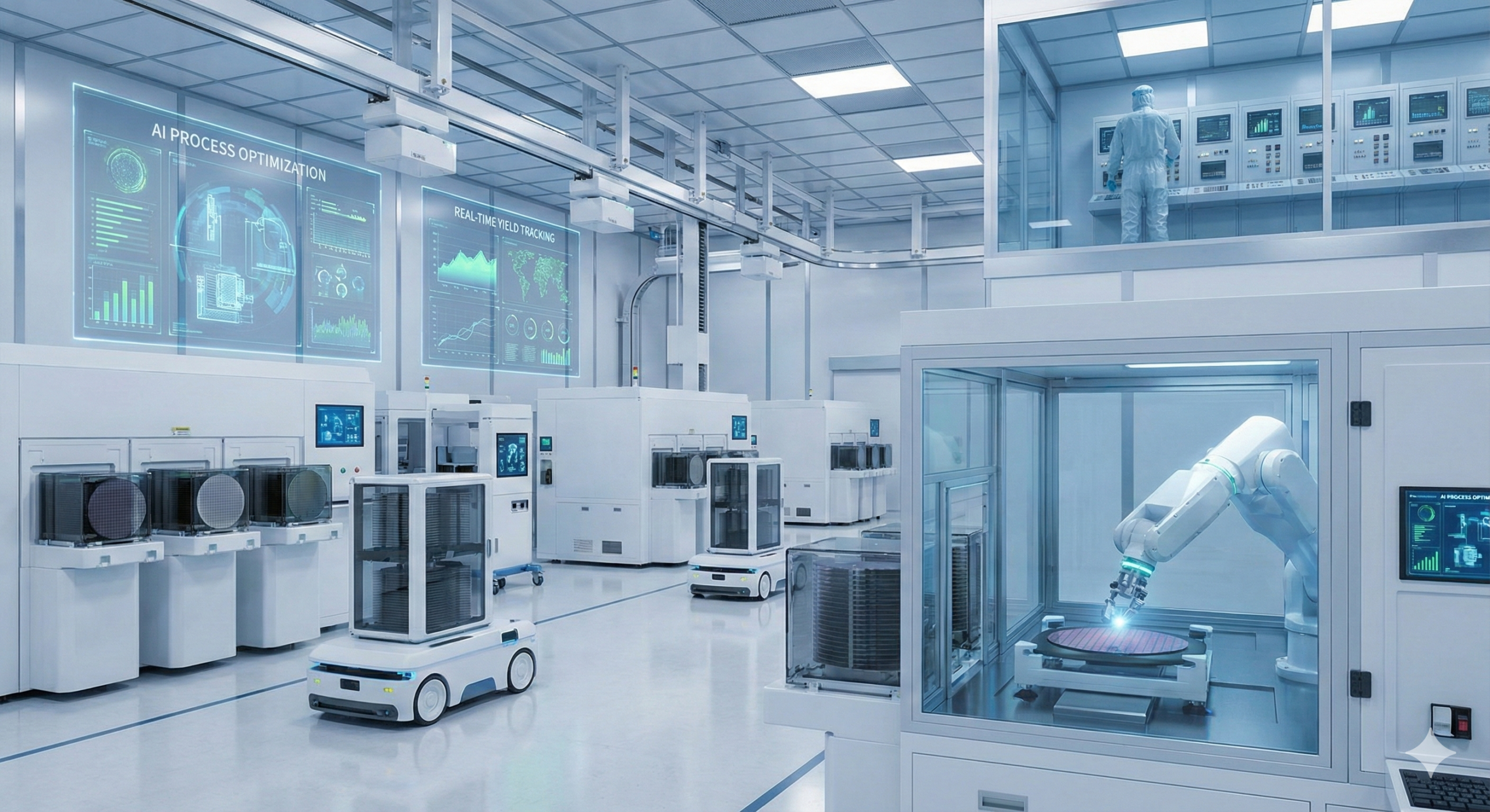
Equipment Control Software: The Brain of the Fab
Equipment control software serves as the digital nervous system of a semiconductor fab. By connecting and orchestrating thousands of tools and sensors, it enables real-time monitoring, seamless communication, and rapid response to process deviations. Modern control software supports standardized communication protocols and integrates with manufacturing execution systems (MES) to provide centralized oversight of fab operations. This level of coordination allows fabs to maintain high levels of throughput, reduce errors, and respond quickly to changes in production schedules or process conditions.
Advanced Process Control: Driving Yield and Process Stability
Advanced Process Control (APC) has emerged as the intelligence layer in semiconductor manufacturing. By leveraging run-to-run control, fault detection, and predictive analytics, APC systems enable fabs to adjust processes in real time to minimize variability and maximize yield. As semiconductor nodes shrink to sub-5nm and beyond, process windows become increasingly narrow, and even minor deviations can result in significant yield losses. APC, often augmented with AI and machine learning, allows fabs to proactively manage these variations, reduce defects, and maintain stable, repeatable processes across high-volume production.
200 mm Fabs: Modernizing Mature Nodes
While 200 mm fabs operate on mature semiconductor nodes, they remain crucial for producing automotive, power management, analog, and IoT chips. Many of these fabs are undergoing modernization, incorporating automation systems to improve throughput, reduce downtime, and extend the lifecycle of existing production lines. By integrating AMHS, robotics, and process control solutions, 200 mm fabs are able to meet growing demand for specialized chips without extensive capital investment in new facilities.
300 mm Fabs: Scaling Advanced Production
300 mm fabs represent the standard for high-volume, leading-edge semiconductor manufacturing. Automation is foundational to these facilities, enabling ultra-clean wafer processing, precise tool coordination, and optimized throughput. As production scales for advanced nodes such as 5 nm, 3 nm, and beyond, automation ensures consistency and reduces variability in processes that are extremely sensitive to environmental and operational conditions. The combination of robotics, material handling systems, and advanced control software allows 300 mm fabs to achieve higher yield and operational efficiency while meeting the stringent demands of global customers.
IDMs, Foundries, and OSATs: Diverse Automation Needs
Integrated Device Manufacturers (IDMs) leverage fab automation to maintain control over proprietary processes, improve efficiency, and accelerate time-to-market. Foundries, which serve multiple clients with varying requirements, depend on automation to scale production flexibly and efficiently, handling high-mix, high-volume workloads. Outsourced Semiconductor Assembly & Test (OSAT) providers are increasingly adopting automation to support advanced packaging technologies, including 2.5D and 3D integration, hybrid bonding, and complex testing processes. Across all segments, automation enables manufacturers to maintain quality, reduce cycle times, and optimize costs.
The Future: Toward Fully Autonomous Fabs
The next evolution in fab automation is defined by digital twins, AI-driven scheduling, predictive maintenance, and autonomous process optimization. By integrating real-time data from equipment, sensors, and metrology systems, fabs can simulate and optimize workflows, anticipate failures, and implement corrective actions without human intervention. The ultimate goal is the fully autonomous fab, where human operators oversee strategy and supervision rather than manual process control. This shift not only improves productivity but also positions manufacturers to meet the exponential growth in chip demand across multiple industries.
As global semiconductor demand surges, fab automation is no longer optional; it is a strategic imperative. Automated material handling, robotics, advanced process control, and integrated control software are transforming how fabs operate, enabling higher yields, faster throughput, and improved operational stability. From modernizing 200 mm fabs to scaling 300 mm advanced-node production, automation is helping IDMs, foundries, and OSATs meet the challenges of the next decade. The winners in this competitive landscape will be those who embrace automation most effectively, driving efficiency, innovation, and sustainability in semiconductor manufacturing.
FAQ
1. What is Fab Automation, and why is it important?
Fab automation refers to the use of advanced technologies—including automated material handling systems (AMHS), robotics, equipment control software, and advanced process control (APC)—to streamline semiconductor fabrication. Automation is critical because modern fabs must handle increasingly complex processes, reduce variability, maximize yield, and meet the surging demand for advanced chips.
2. What is driving growth in the Fab Automation Market?
The market is fueled by several factors:
- Growing demand for AI, HPC, automotive, 5G, and IoT chips.
- Expansion of 300 mm advanced-node fabs and modernization of 200 mm mature-node fabs.
- Rising focus on yield improvement, throughput enhancement, and contamination control.
- Adoption of AI-driven process control and digital twins for predictive and autonomous operations.
3. Which technologies dominate the Fab Automation Market?
Key technologies include:
- Automated Material Handling Systems (AMHS) – ensuring precise wafer movement.
- Robotics & Handling Equipment – performing delicate and repeatable tasks.
- Equipment Control Software – enabling real-time monitoring and tool orchestration.
- Advanced Process Control (APC) – optimizing processes for yield and consistency.
4. How do wafer sizes (200 mm vs. 300 mm) influence automation adoption?
200 mm fabs, which produce automotive, analog, and IoT chips, are increasingly modernizing with automation to extend their lifecycle and improve efficiency. 300 mm fabs, typically handling high-volume, advanced-node production, rely heavily on full automation for throughput, process stability, and yield management. Investors should note that 300 mm fabs represent the largest growth segment in automation adoption.
5. How does the market vary by customer type?
- IDMs (Integrated Device Manufacturers) adopt automation to maintain vertical integration and control over proprietary processes.
- Foundries require scalable, flexible automation to serve multiple clients with diverse production needs.
- OSATs (Outsourced Semiconductor Assembly & Test) implement automation to handle advanced packaging technologies, including 2.5D and 3D integration.
About MarketsandMarkets™
MarketsandMarkets™ has been recognized as one of America’s Best Management Consulting Firms by Forbes, as per their recent report.
MarketsandMarkets™ is a blue ocean alternative in growth consulting and program management, leveraging a man-machine offering to drive supernormal growth for progressive organizations in the B2B space. With the widest lens on emerging technologies, we are proficient in co-creating supernormal growth for clients across the globe.
Today, 80% of Fortune 2000 companies rely on MarketsandMarkets, and 90 of the top 100 companies in each sector trust us to accelerate their revenue growth. With a global clientele of over 13,000 organizations, we help businesses thrive in a disruptive ecosystem.
The B2B economy is witnessing the emergence of $25 trillion in new revenue streams that are replacing existing ones within this decade. We work with clients on growth programs, helping them monetize this $25 trillion opportunity through our service lines – TAM Expansion, Go-to-Market (GTM) Strategy to Execution, Market Share Gain, Account Enablement, and Thought Leadership Marketing.
Built on the ‘GIVE Growth’ principle, we collaborate with several Forbes Global 2000 B2B companies to keep them future-ready. Our insights and strategies are powered by industry experts, cutting-edge AI, and our Market Intelligence Cloud, KnowledgeStore™, which integrates research and provides ecosystem-wide visibility into revenue shifts.
To find out more, visit www.MarketsandMarkets™.com or follow us on Twitter , LinkedIn and Facebook .
Contact:
Mr. Rohan Salgarkar
MarketsandMarkets™ INC.
1615 South Congress Ave.
Suite 103, Delray Beach, FL 33445
USA: +1-888-600-6441
Visit Our Website: https://www.marketsandmarkets.com/