The hybrid bonding market is emerging as one of the most transformative segments in advanced semiconductor packaging. Once considered a niche innovation used in specialized applications, hybrid bonding is now rapidly evolving into a mainstream enabler of 3D integration, chiplet architectures, and next-generation high-performance computing systems.
According to a MarketsandMarkets report, the hybrid bonding market is projected to grow from USD 164.7 million in 2025 to USD 633.9 million by 2032, registering a strong CAGR of 21.2% during the forecast period. This growth reflects the semiconductor industry’s structural shift toward ultra-dense interconnects, advanced packaging, and heterogeneous integration.
1. Transition from Scaling Limits to 3D Integration
Traditional semiconductor scaling approaches are reaching physical and economic limits. As transistor scaling slows, the industry is increasingly relying on 3D stacking and advanced packaging to enhance performance.
Hybrid bonding enables direct copper-to-copper and dielectric-to-dielectric connections without solder bumps, significantly improving:
- Interconnect density
- Signal integrity
- Power efficiency
- Bandwidth performance
This makes it a foundational technology for overcoming the limitations of Moore’s Law through system-level scaling.
2. AI and High-Performance Computing Driving Demand
One of the strongest growth drivers for hybrid bonding is the explosive demand from AI accelerators and high-performance computing (HPC) workloads.
Modern AI systems require:
- Extremely high memory bandwidth
- Low-latency data transfer between logic and memory
- Dense 3D integration of compute units
Hybrid bonding directly addresses these requirements by enabling tight vertical integration of memory and logic dies, making it critical for next-generation AI chips, GPUs, and data center processors.
3. Chiplet Architecture Accelerating Adoption
The semiconductor industry is rapidly shifting toward chiplet-based design, where complex systems are broken into smaller, modular dies and integrated together.
Hybrid bonding plays a key role by enabling:
- Ultra-fine pitch interconnects
- High-density die-to-die connectivity
- Improved yield through modular manufacturing
- Flexible system design across process nodes
As chiplet ecosystems expand, hybrid bonding is becoming the preferred interconnect technology for heterogeneous integration.
4. Memory Innovation: High Bandwidth Memory (HBM) and Beyond
Advanced memory technologies, especially High Bandwidth Memory (HBM), are a major catalyst for hybrid bonding adoption.
Memory manufacturers are leveraging hybrid bonding to:
- Stack multiple DRAM layers with higher density
- Increase bandwidth between memory and compute units
- Reduce power consumption per bit transfer
This is particularly important for AI workloads, where memory bandwidth is often the primary bottleneck.
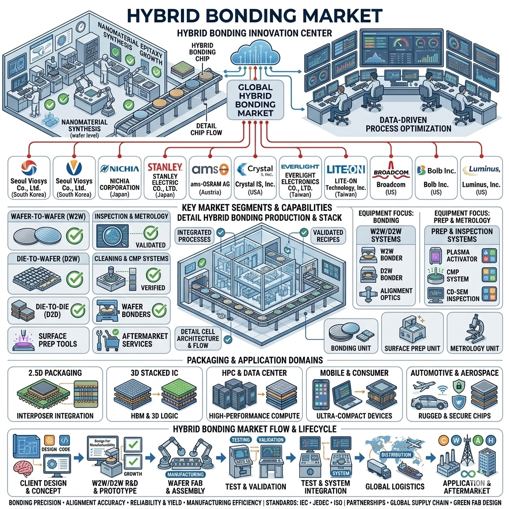
5. Equipment and Ecosystem Expansion
The growth of hybrid bonding is also accelerating demand for specialized semiconductor equipment, including:
- Wafer bonders
- Surface preparation tools
- Inspection and metrology systems
- Cleaning and planarization equipment
Leading semiconductor equipment vendors are heavily investing in improving precision alignment, defect control, and throughput scalability, enabling hybrid bonding to move into high-volume manufacturing environments.
Download PDF Brochure @ https://www.marketsandmarkets.com/pdfdownloadNew.asp?id=2641237
6. Regional Leadership: Asia Pacific at the Core
Asia Pacific dominates the hybrid bonding ecosystem due to its concentration of:
- Leading foundries
- Memory manufacturers
- Advanced packaging facilities
Countries such as Taiwan, South Korea, Japan, and China are investing heavily in 3D integration capabilities and semiconductor packaging infrastructure, making the region the global hub for hybrid bonding adoption.
7. Key Industry Shift: From Innovation to Standardization
Perhaps the most important trend is the transition of hybrid bonding from R&D-driven innovation to production-scale deployment.
Recent industry momentum shows increasing adoption in:
- AI chip manufacturing
- Advanced memory stacking
- 2.5D and 3D IC packaging
- High-performance logic integration
Even equipment suppliers are reporting rising orders tied to hybrid bonding adoption in AI-related applications, signaling accelerating commercialization.
Conclusion: A Foundational Technology for the Next Semiconductor Era
Hybrid bonding is no longer an experimental packaging technique—it is becoming a core enabling technology for the future of semiconductors.
As the industry moves toward:
- 3D integration
- Chiplet-based architectures
- AI-driven compute systems
- Advanced memory scaling
Hybrid bonding is positioned at the center of this transformation.
With strong growth projections, increasing industrial adoption, and rapid ecosystem development, the technology is clearly transitioning from niche innovation to industry standard—defining the next era of semiconductor advancement.
About MarketsandMarkets™
MarketsandMarkets™ has been recognized as one of America’s Best Management Consulting Firms by Forbes, as per their recent report.
MarketsandMarkets™ is a blue ocean alternative in growth consulting and program management, leveraging a man-machine offering to drive supernormal growth for progressive organizations in the B2B space. With the widest lens on emerging technologies, we are proficient in co-creating supernormal growth for clients across the globe.
Today, 80% of Fortune 2000 companies rely on MarketsandMarkets, and 90 of the top 100 companies in each sector trust us to accelerate their revenue growth. With a global clientele of over 13,000 organizations, we help businesses thrive in a disruptive ecosystem.
The B2B economy is witnessing the emergence of $25 trillion in new revenue streams that are replacing existing ones within this decade. We work with clients on growth programs, helping them monetize this $25 trillion opportunity through our service lines – TAM Expansion, Go-to-Market (GTM) Strategy to Execution, Market Share Gain, Account Enablement, and Thought Leadership Marketing.
Built on the ‘GIVE Growth’ principle, we collaborate with several Forbes Global 2000 B2B companies to keep them future-ready. Our insights and strategies are powered by industry experts, cutting-edge AI, and our Market Intelligence Cloud, KnowledgeStore™, which integrates research and provides ecosystem-wide visibility into revenue shifts.
To find out more, visit www.MarketsandMarkets™.com or follow us on Twitter , LinkedIn and Facebook .
Contact:
Mr. Rohan Salgarkar
MarketsandMarkets™ INC.
1615 South Congress Ave.
Suite 103, Delray Beach, FL 33445
USA: +1-888-600-6441