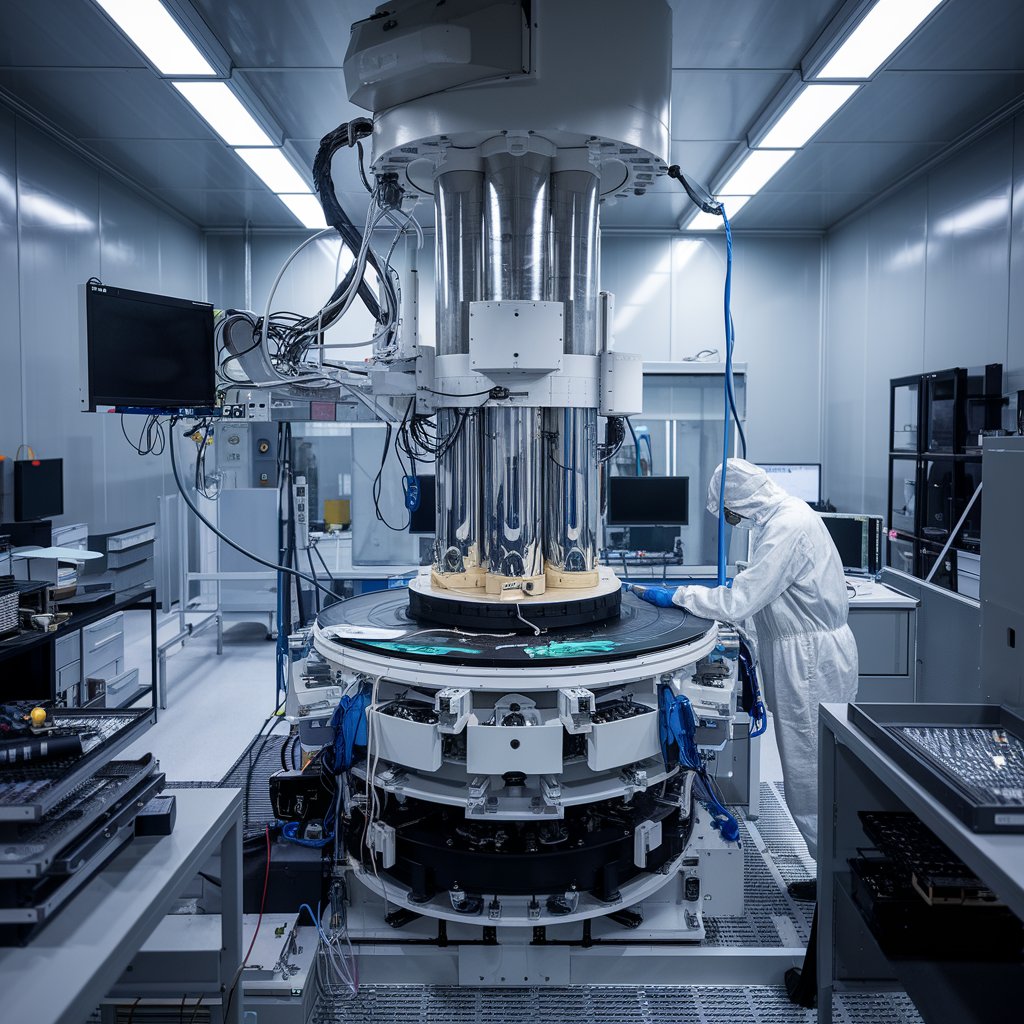
The United States’ role in the global Extreme Ultraviolet (EUV) lithography ecosystem has become increasingly strategic as demand for advanced semiconductors grows exponentially. EUV lithography, a next-generation chip manufacturing technology that uses light with a wavelength of 13.5 nanometers, is critical for producing the most advanced logic and memory chips at 5nm, 3nm, and even smaller nodes. Although ASML of the Netherlands dominates EUV tool manufacturing, the U.S. plays a pivotal role through its dominance in key subsystems, materials, and intellectual property.
The U.S. Role in the Global EUV Ecosystem
While the Netherlands-based company ASML is the sole manufacturer of EUV lithography systems, the United States plays a critical role in supporting this technology. American companies are key suppliers of core components and technologies that enable EUV tools to function. Cymer, a U.S. company and subsidiary of ASML, provides the high-powered laser light source technology that drives EUV systems. U.S. companies such as KLA and Applied Materials supply essential tools for wafer inspection, etching, and metrology, which are necessary for the EUV process. Additionally, the U.S. leads in software for chip design through firms like Synopsys and Cadence, whose tools are adapted specifically for EUV-era design complexity.
Materials and Chemicals Innovationa
Photoresists, pellicles, and other advanced materials are vital for successful EUV lithography. U.S. companies, including DuPont and Inpria (headquartered in the U.S. before being acquired by JSR), are at the forefront of developing high-sensitivity EUV photoresists that ensure accuracy and yield. These materials are engineered to withstand high-energy EUV exposure while maintaining pattern fidelity. The development of pellicles—protective membranes used to keep masks free of contamination during EUV exposure—is another area where U.S. R&D is contributing to overcoming one of EUV’s biggest operational hurdles.
Download PDF Brochure @ https://www.marketsandmarkets.com/pdfdownloadNew.asp?id=241564826
Government Support and Strategic Funding
Recognizing the strategic importance of semiconductors, the U.S. government enacted the CHIPS and Science Act in 2022, allocating more than $50 billion to revitalize domestic chip manufacturing. A significant portion of this funding is directed toward advanced node manufacturing that requires EUV technology. Companies like Intel are receiving federal and state-level support to build and expand EUV-capable fabs in Arizona, Ohio, and New Mexico. These efforts aim not only to reduce reliance on overseas fabs but also to ensure that the U.S. can manufacture cutting-edge chips for both commercial and defense applications.
Geopolitical Dynamics and Export Controls
EUV technology has also become a focal point in the geopolitical struggle between the U.S. and China. Due to national security concerns, the U.S., along with allies such as the Netherlands and Japan, has imposed strict export controls to prevent the transfer of advanced semiconductor manufacturing technology to China. These measures include restrictions on the sale of EUV scanners and even advanced DUV tools. The goal is to limit China’s ability to produce leading-edge chips domestically, thereby preserving the West’s technological advantage.
High-NA EUV and the Next Phase of Innovation
The next generation of EUV technology, known as High-NA (Numerical Aperture), promises even greater resolution for chip patterning at the 2nm scale and beyond. ASML is already developing these systems, and U.S. companies are contributing critical innovations in optics, materials, and software modeling. High-NA EUV will allow smaller features, better image contrast, and improved process windows, but it will also require new photoresist chemistries and inspection tools—areas where U.S. expertise will be instrumental.
Workforce Development and Education
One of the major challenges facing the U.S. EUV industry is the shortage of specialized talent. Operating and maintaining EUV tools requires skills in laser physics, materials science, and vacuum systems. Recognizing this, government and industry have launched initiatives with universities, community colleges, and technical training centers to build a pipeline of skilled engineers and technicians. These programs are essential to support the growing number of EUV-equipped facilities being built domestically.
Challenges and Strategic Risks
Despite its strengths, the U.S. faces several vulnerabilities. It is still dependent on ASML for complete EUV systems and on global supply chains for key components. EUV machines are complex and extremely expensive, with each system costing over $150 million and requiring 12–18 months to build and ship. Throughput and defect control also remain technical hurdles in full-scale EUV deployment. Addressing these issues will require continued investment in R&D, infrastructure, and workforce development.
Future Outlook
Looking ahead, the U.S. is well-positioned to strengthen its influence in the EUV lithography space. With significant federal investment, robust private-sector innovation, and strong alliances with key global partners, the U.S. can play a central role in the evolution of semiconductor manufacturing. As High-NA EUV becomes a reality and demand for advanced chips accelerates, the integration of U.S. expertise in materials, optics, software, and metrology will become even more critical. The coming decade presents an opportunity for the U.S. not only to lead in EUV but also to shape the global semiconductor landscape.
About MarketsandMarkets™
MarketsandMarkets™ has been recognized as one of America’s Best Management Consulting Firms by Forbes, as per their recent report.
MarketsandMarkets™ is a blue ocean alternative in growth consulting and program management, leveraging a man-machine offering to drive supernormal growth for progressive organizations in the B2B space. With the widest lens on emerging technologies, we are proficient in co-creating supernormal growth for clients across the globe.
Today, 80% of Fortune 2000 companies rely on MarketsandMarkets, and 90 of the top 100 companies in each sector trust us to accelerate their revenue growth. With a global clientele of over 13,000 organizations, we help businesses thrive in a disruptive ecosystem.
The B2B economy is witnessing the emergence of $25 trillion in new revenue streams that are replacing existing ones within this decade. We work with clients on growth programs, helping them monetize this $25 trillion opportunity through our service lines – TAM Expansion, Go-to-Market (GTM) Strategy to Execution, Market Share Gain, Account Enablement, and Thought Leadership Marketing.
Built on the ‘GIVE Growth’ principle, we collaborate with several Forbes Global 2000 B2B companies to keep them future-ready. Our insights and strategies are powered by industry experts, cutting-edge AI, and our Market Intelligence Cloud, KnowledgeStore™, which integrates research and provides ecosystem-wide visibility into revenue shifts.
To find out more, visit www.MarketsandMarkets™.com or follow us on Twitter , LinkedIn and Facebook .
Contact:
Mr. Rohan Salgarkar
MarketsandMarkets™ INC.
1615 South Congress Ave.
Suite 103, Delray Beach, FL 33445
USA: +1-888-600-6441
Visit Our Website: https://www.marketsandmarkets.com/