The semiconductor industry is at a pivotal juncture, fueled by transformative technologies such as artificial intelligence, 5G connectivity, autonomous vehicles, and quantum computing. As the need for more powerful, compact, and energy-efficient chips intensifies, Extreme Ultraviolet Lithography (EUVL) has emerged as the most critical enabler of next-generation semiconductor manufacturing. The EUVL industry is not only gaining momentum—it is becoming the backbone of global chip innovation.
EUVL: The Core Technology for Advanced Nodes
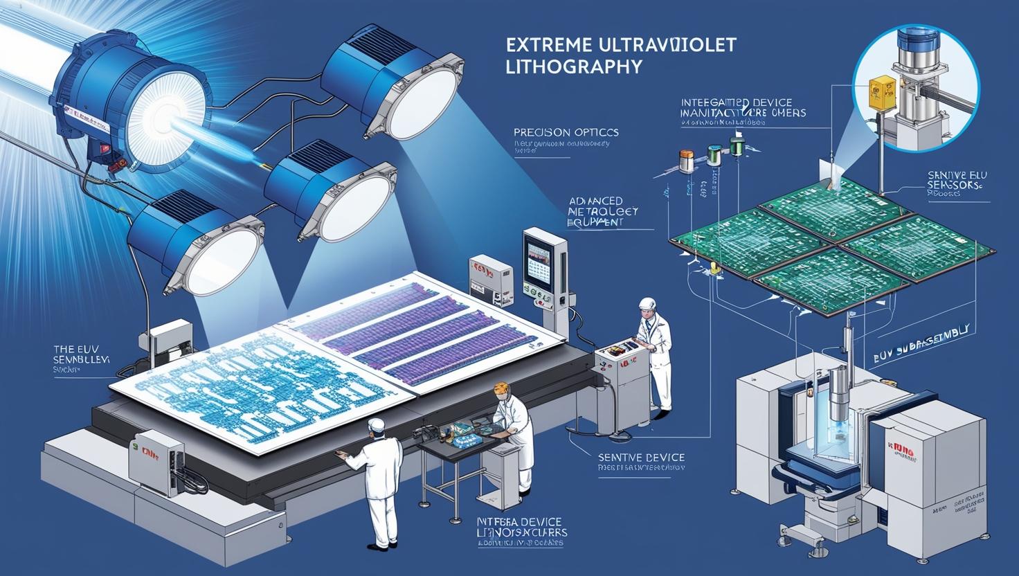
EUVL uses a 13.5-nanometer wavelength light source—significantly shorter than the deep ultraviolet (DUV) lithography’s 193-nanometer wavelength—to print ultra-fine circuit patterns on silicon wafers. This technological advancement allows chipmakers to produce transistors at geometries smaller than 7 nanometers, such as 5nm, 3nm, and even 2nm nodes, with greater efficiency and precision. Compared to multi-patterning methods used in DUV, EUVL reduces process complexity, improves yield, and supports higher transistor densities—all of which are vital for today’s increasingly complex chip architectures.
Industry Leaders and Technology Suppliers
The EUVL industry is heavily driven by a few dominant players, most notably ASML, the only company currently capable of producing commercial EUV lithography machines. ASML’s latest innovations, including its High Numerical Aperture (High-NA) EUV systems, are designed to push patterning resolution even further, allowing semiconductor manufacturers to move into sub-2nm territory. The EUV lithography market is expected to reach USD 22.69 billion by 2029 from USD 12.18 billion in 2024, at a CAGR of 13.2% during the 2024-2029 period.
Companies like Taiwan Semiconductor Manufacturing Company (TSMC), Samsung Foundry, and Intel are already incorporating EUVL into their advanced manufacturing processes. These firms are investing billions of dollars in expanding EUV-based fabrication capacity across Asia, North America, and Europe. Their aggressive roadmaps and capital expenditure plans reflect a firm commitment to EUVL as the core technology for the decade ahead.
Download PDF Brochure @ https://www.marketsandmarkets.com/pdfdownloadNew.asp?id=241564826
Demand Fueled by AI, Data Centers, and Edge Devices
The acceleration in EUVL adoption is largely driven by an explosion of data and computing needs. Generative AI, in particular, has created a surge in demand for powerful chips capable of handling vast neural network computations. EUV-based chips offer the transistor density and power efficiency necessary to support high-performance AI accelerators, graphics processors, and custom system-on-chip (SoC) designs.
Simultaneously, the rapid rollout of 5G infrastructure, the rise of Internet of Things (IoT) ecosystems, and increased deployment of edge computing solutions are pressuring the industry to deliver chips with greater performance-per-watt efficiency. EUVL is uniquely positioned to meet these requirements by enabling the creation of smaller, faster, and more energy-efficient processors.
Investment Surge and Supply Chain Challenges
The global rush toward EUV technology has spurred record levels of investment from both private companies and national governments. Semiconductor manufacturers are expanding their cleanroom capacity and entering long-term agreements with equipment suppliers to secure access to EUV tools. The U.S. CHIPS and Science Act, EU Chips Act, and similar initiatives in Japan and South Korea are injecting billions of dollars into domestic semiconductor ecosystems, with EUV infrastructure as a top priority.
However, the industry’s growth is not without hurdles. The production of EUV machines requires an intricate, highly specialized supply chain. Critical components such as Zeiss’s optical systems, light source modules from Cymer (ASML-owned), and specialized resists and photomasks are manufactured by a handful of companies. This limited supplier pool introduces bottlenecks that can constrain system availability and delay fab expansion timelines.
Moreover, the steep learning curve associated with EUV process development demands a highly skilled workforce. As fabs adopt increasingly sophisticated patterning techniques, there is a growing shortage of engineers and technicians trained in EUV-specific operations—an issue that chipmakers and governments are scrambling to address through talent development programs and academic-industry partnerships.
The Future of EUVL: High-NA and Beyond
Looking forward, the EUVL industry is preparing for a second wave of innovation with the deployment of High-NA EUV systems, which offer greater resolution through increased numerical aperture optics. These systems are critical for patterning beyond the 2nm node and are expected to be introduced in pilot production lines as early as 2026. Alongside hardware advancements, new developments in resist materials, photomask durability, and lithography simulation software will enhance the overall efficiency and scalability of EUV technology.
As the world becomes more digitally interconnected and AI-driven, the need for increasingly capable chips will only intensify. The EUVL industry, standing at the crossroads of optical physics, nanotechnology, and precision engineering, is poised to play a defining role in shaping the future of global innovation.
Extreme Ultraviolet Lithography is no longer a futuristic promise—it is today’s reality and tomorrow’s necessity. As the semiconductor sector grapples with ever-increasing complexity and scale, EUVL provides the only viable path forward for sustained miniaturization and performance gains. With accelerating demand, intensifying investment, and continuous innovation, the EUVL industry is set to become the linchpin of advanced semiconductor manufacturing for years to come.
About MarketsandMarkets™
MarketsandMarkets™ is a blue ocean alternative in growth consulting and program management, leveraging a man-machine offering to drive supernormal growth for progressive organizations in the B2B space. We have the widest lens on emerging technologies, making us proficient in co-creating supernormal growth for clients.
The B2B economy is witnessing the emergence of $25 trillion of new revenue streams that are substituting existing revenue streams in this decade alone. We work with clients on growth programs, helping them monetize this $25 trillion opportunity through our service lines – TAM Expansion, Go-to-Market (GTM) Strategy to Execution, Market Share Gain, Account Enablement, and Thought Leadership Marketing.
Built on the ’GIVE Growth’ principle, we work with several Forbes Global 2000 B2B companies – helping them stay relevant in a disruptive ecosystem. Our insights and strategies are molded by our industry experts, cutting-edge AI-powered Market Intelligence Cloud, and years of research. The KnowledgeStore™ (our Market Intelligence Cloud) integrates our research, facilitates an analysis of interconnections through a set of applications, helping clients look at the entire ecosystem and understand the revenue shifts happening in their industry.
To find out more, visit www.MarketsandMarkets™.com or follow us on Twitter, LinkedIn and Facebook.
Contact:
Mr. Rohan Salgarkar
MarketsandMarkets™ INC.
1615 South Congress Ave.
Suite 103
Delray Beach, FL 33445
USA : 1-888-600-6441