The semiconductor industry is undergoing a transformative shift as demand for smaller, faster, and more power-efficient chips continues to accelerate. At the heart of this evolution is Extreme Ultraviolet Lithography (EUVL)—a cutting-edge photolithography technology enabling the production of advanced semiconductor nodes below 7 nanometers. EUVL is fast becoming a cornerstone of next-generation chip fabrication, driving substantial growth in its global market.
EUV Lithography: Powering the Future of Semiconductor Innovation
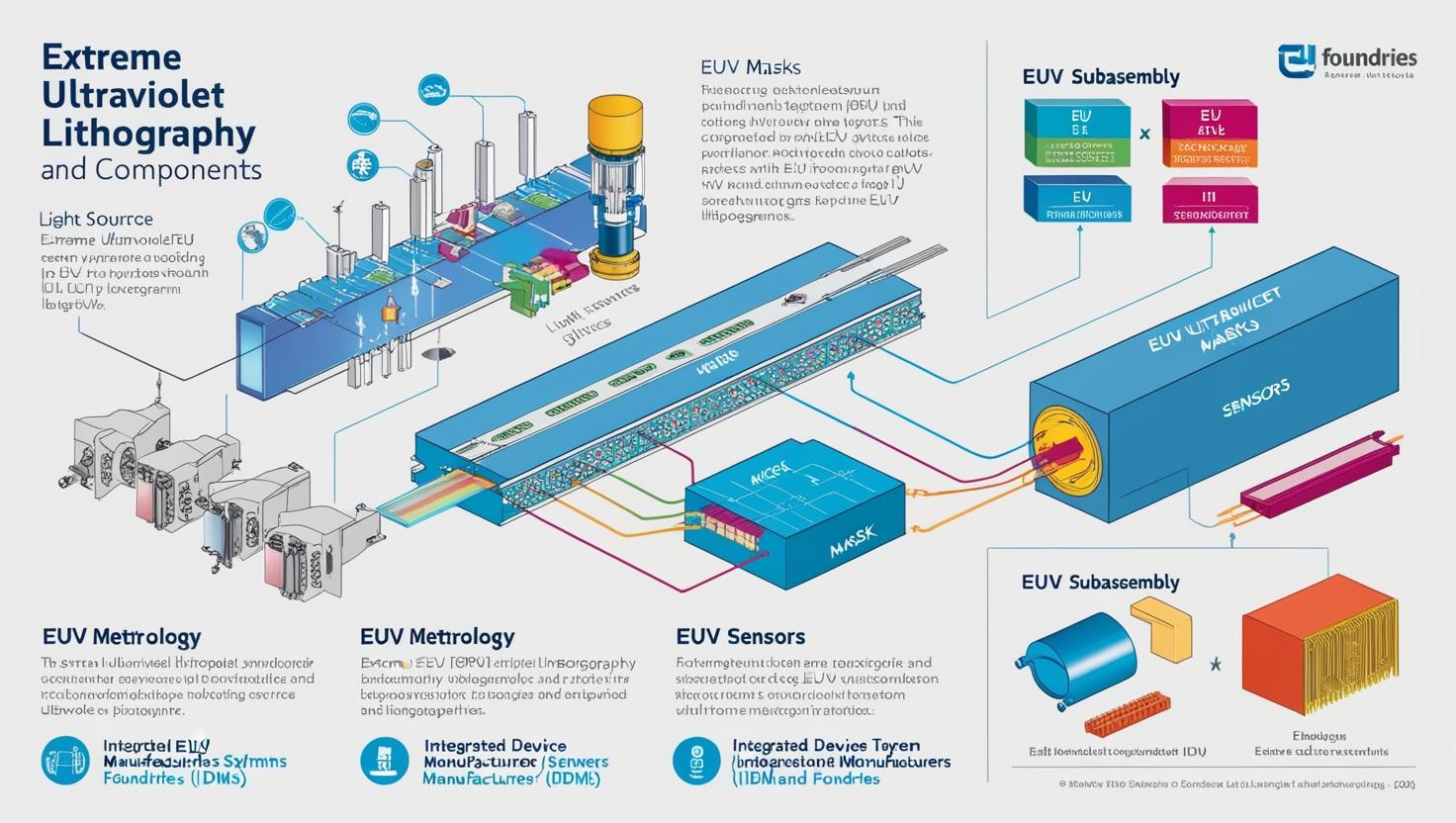
Extreme Ultraviolet Lithography utilizes light with extremely short wavelengths (13.5 nanometers) to print intricate patterns on silicon wafers with extraordinary precision. Unlike conventional deep ultraviolet (DUV) lithography, EUVL allows for fewer multi-patterning steps, enabling more accurate and cost-effective production of sub-7nm and even sub-3nm nodes.
This capability is critical for enabling advanced computing workloads, from artificial intelligence (AI) and 5G networks to autonomous vehicles and edge computing. As industries shift toward high-performance and energy-efficient systems, EUVL has emerged as a pivotal technology in overcoming the limitations of traditional lithography.
Foundry Investments and Capacity Expansion Drive Demand
Semiconductor giants such as TSMC, Intel, and Samsung are heavily investing in EUVL systems to remain competitive in the global chip race. The adoption of 3nm and 2nm process technologies has become a strategic imperative, with these advanced nodes relying almost entirely on EUV systems for production.
ASML—the sole provider of EUV lithography machines—has seen a surge in orders as leading foundries ramp up capacity. Represents a significant capital commitment, but one that enables manufacturers to produce faster, smaller, and more power-efficient chips at scale.
EUVL adoption is expanding beyond top-tier foundries to include IDMs (Integrated Device Manufacturers) and new players in Asia-Pacific and the Middle East.
Global Supply Chain Expansion and Regional Growth
While the technology was initially concentrated in a few regions, particularly the U.S., South Korea, Taiwan, and the Netherlands, the EUVL market is seeing geographic diversification. Countries like China, India, and Saudi Arabia are investing in local semiconductor ecosystems, including EUV capabilities, to strengthen technological self-sufficiency and reduce reliance on global supply chains.
This expansion is expected to drive regional growth in EUVL equipment, services, and materials, fueling demand for photomasks, pellicles, photoresists, and optics that support EUV processes.
Download PDF Brochure @ https://www.marketsandmarkets.com/pdfdownloadNew.asp?id=241564826
Technology Trends: From High-NA EUV to Yield Optimization
The next evolution in EUV technology—High-NA (Numerical Aperture) EUV—is already underway. High-NA EUV offers greater resolution and tighter line widths, allowing for even more advanced nodes (beyond 2nm). ASML’s High-NA EUV systems are being tested by early adopters and are expected to enter production in the next few years.
In parallel, advancements in metrology, defect inspection, and process control are being integrated with EUV lithography to improve yield rates and manufacturing efficiency. These enhancements are essential for reducing costs and making EUV viable for a wider range of applications beyond flagship processors and GPUs.
Applications Beyond Logic Chips
While logic chips (CPUs and GPUs) are the primary beneficiaries of EUVL, the technology is also extending into other domains:
Memory Devices (DRAM and NAND): EUV is being evaluated for patterning critical layers in next-gen memory technologies to improve performance and density.
AI Accelerators: Specialized chips for machine learning and data centers rely on high transistor counts, benefiting from EUVL’s fine patterning capabilities.
Automotive Semiconductors: Advanced driver assistance systems (ADAS) and autonomous vehicles require high-reliability, high-performance chips that EUVL can help fabricate.
Challenges and Considerations
Despite its promise, EUV lithography still faces a number of challenges:
High Equipment Costs: EUV scanners are among the most expensive tools in a fab, which can limit adoption among smaller players.
Complex Infrastructure Requirements: EUV systems require a cleanroom environment, advanced cooling systems, and precision optics.
Mask Defects and Pellicle Limitations: Ensuring defect-free masks and durable pellicles is critical to maintaining production yield.
However, continuous R&D and collaboration among ecosystem players are helping overcome these barriers, making EUV more accessible over time.

Market Outlook: Strong Growth Ahead
According to industry analysts, the EUV lithography market is expected to grow at a CAGR of over 13.2% through 2029, fueled by ongoing semiconductor innovation and manufacturing expansion. ASML, the dominant equipment supplier, projects continued revenue growth as demand for both EUV and future High-NA systems increases.
In tandem with global digitalization trends, EUVL is not just a niche technology—it is becoming a mainstream enabler of the entire chip industry’s future.
Opportunities in the EUVL Market
Adoption in Advanced Node Manufacturing (3nm and Beyond)
With global chipmakers transitioning to 3nm and 2nm nodes, EUV lithography is becoming essential for patterning ultra-small features. This creates strong demand for EUV systems and supporting materials across foundries and integrated device manufacturers (IDMs).
High-NA EUV Technology Rollout
The development of High Numerical Aperture (High-NA) EUV represents a major leap forward in resolution and performance. Companies investing early in High-NA systems stand to gain a competitive edge in manufacturing future nodes like 1.4nm and beyond.
Expansion into Memory and AI Chip Production
While EUV has primarily been used for logic chips, it’s now being adopted for DRAM and NAND memory as well as AI accelerators, opening new vertical markets for EUV tools and photoresists.
Emerging Semiconductor Hubs in Asia & Middle East
Countries like India, China, Vietnam, and Saudi Arabia are developing their own chip manufacturing ecosystems. As they build advanced fabs, there’s growing opportunity for EUV system suppliers and support services.
Growth in Materials and Subsystems Markets
EUV lithography relies on a specialized ecosystem of masks, pellicles, resists, mirrors, and optics. Suppliers of these materials and subsystems have an opportunity to scale alongside the rise in EUV machine shipments.
Support Services and EUV Ecosystem Development
With EUV systems requiring complex installation, calibration, and maintenance, there’s rising demand for engineering support, metrology solutions, and EUV process control tools, especially in newly established fabs.
Collaborations with AI, HPC, and Automotive Chipmakers
As AI, high-performance computing (HPC), and automotive electronics evolve, chipmakers in these domains will increasingly adopt EUV. Strategic collaborations with these industries present long-term growth avenues.
Conclusion: EUVL at the Core of Semiconductor Advancement
Extreme Ultraviolet Lithography is no longer an experimental technology; it is a commercial necessity. As the world enters the era of ultra-miniaturized electronics, AI workloads, and ubiquitous connectivity, EUVL is laying the foundation for a new generation of silicon innovation.
With ongoing investments, rapid regional adoption, and breakthrough advancements in High-NA lithography, the EUVL market is poised for unprecedented growth, reshaping the landscape of semiconductor manufacturing for years to come.
About MarketsandMarkets™
MarketsandMarkets™ is a blue ocean alternative in growth consulting and program management, leveraging a man-machine offering to drive supernormal growth for progressive organizations in the B2B space. We have the widest lens on emerging technologies, making us proficient in co-creating supernormal growth for clients.
The B2B economy is witnessing the emergence of $25 trillion of new revenue streams that are substituting existing revenue streams in this decade alone. We work with clients on growth programs, helping them monetize this $25 trillion opportunity through our service lines – TAM Expansion, Go-to-Market (GTM) Strategy to Execution, Market Share Gain, Account Enablement, and Thought Leadership Marketing.
Built on the ’GIVE Growth’ principle, we work with several Forbes Global 2000 B2B companies – helping them stay relevant in a disruptive ecosystem. Our insights and strategies are molded by our industry experts, cutting-edge AI-powered Market Intelligence Cloud, and years of research. The KnowledgeStore™ (our Market Intelligence Cloud) integrates our research, facilitates an analysis of interconnections through a set of applications, helping clients look at the entire ecosystem and understand the revenue shifts happening in their industry.
To find out more, visit www.MarketsandMarkets™.com or follow us on Twitter, LinkedIn and Facebook.
Contact:
Mr. Rohan Salgarkar
MarketsandMarkets™ INC.
630 Dundee Road
Suite 430
Northbrook, IL 60062
USA : 1-888-600-6441