The rapid expansion of artificial intelligence (AI), cloud computing, and hyperscale data centers is transforming the semiconductor industry, placing advanced chip packaging at the center of next-generation computing innovation. As data center operators demand higher processing performance, faster data transfer, improved energy efficiency, and greater computing density, traditional semiconductor packaging approaches are increasingly facing limitations.
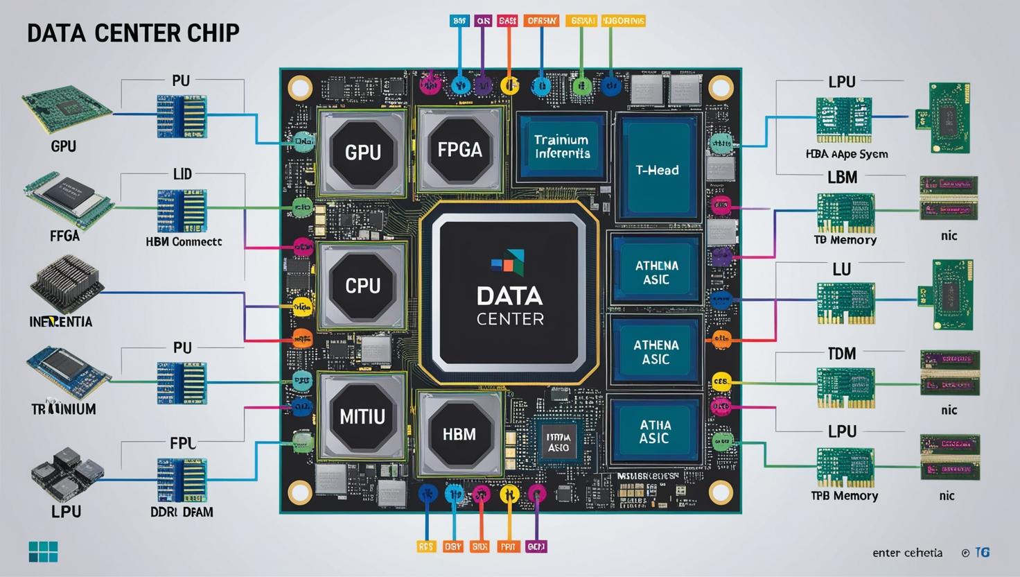
Advanced packaging is emerging as a strategic priority for data center chip manufacturers because it enables multiple semiconductor components, including processors, memory units, and networking elements, to be integrated into compact, high-performance packages. Technologies such as chiplets, 2.5D packaging, 3D stacking, and high-bandwidth memory (HBM) integration are helping semiconductor companies develop powerful computing solutions to support increasingly complex workloads.
According to MarketsandMarkets, the global data center chip market is projected to grow from USD 283.16 billion in 2026 to USD 687.65 billion by 2032, registering a compound annual growth rate (CAGR) of 15.9% during 2026–2032. The growing adoption of AI, machine learning, cloud services, and data-intensive applications is driving demand for high-performance and energy-efficient chips, creating favorable opportunities for advanced packaging technologies.
AI Workloads Increase the Need for Advanced Chip Integration
The growing deployment of generative AI, large language models (LLMs), and machine learning applications is significantly increasing the computational requirements of modern data centers. AI workloads require substantial processing power, high memory bandwidth, and rapid communication between computing components.
Advanced packaging helps address these requirements by bringing multiple chips and memory components closer together within a single package. This approach can reduce interconnect distances, improve communication efficiency, and support higher overall system performance.
For AI accelerators and GPUs, integrating high-bandwidth memory with processing units is particularly important. These configurations allow processors to access large volumes of data more efficiently, supporting demanding AI training and inference workloads.
As hyperscale data centers continue investing in AI infrastructure, advanced packaging is becoming an important consideration in the development of next-generation processors and accelerators.
Chiplet Architecture Reshapes Data Center Chip Design
Chiplet-based architecture is gaining importance as semiconductor manufacturers seek alternatives to increasingly complex monolithic chip designs. Instead of manufacturing an entire processor on a single large silicon die, chiplet architectures divide computing functions into smaller specialized dies that are integrated into a single package.
This approach offers several potential advantages, including improved manufacturing flexibility, better yield management, design scalability, and the ability to combine different semiconductor technologies.
For data center applications, chiplets can integrate CPU cores, AI accelerators, memory controllers, and input/output components within a unified architecture. Manufacturers can also customize chip configurations according to specific workload requirements.
As demand for specialized AI processors and custom data center chips increases, chiplet-based designs are expected to play a greater role in semiconductor innovation.
High-Bandwidth Memory Integration Drives Packaging Innovation
Memory bandwidth has become a critical performance factor in AI and high-performance computing systems. Advanced processors require continuous access to large datasets, and conventional memory architectures can create bottlenecks that limit overall computing efficiency.
High-bandwidth memory (HBM) addresses this challenge by stacking multiple memory dies vertically and connecting them through advanced interconnect technologies. When integrated alongside processors and AI accelerators using advanced packaging, HBM can provide high memory bandwidth within a compact footprint.
The growing adoption of HBM in AI servers and high-performance computing platforms is encouraging semiconductor manufacturers to invest in advanced packaging capabilities.
According to MarketsandMarkets, the memory segment of the data center chip market is expected to register the highest CAGR of 16.7% during the forecast period. This growth highlights the increasing importance of memory technologies in next-generation data center infrastructure.
Download PDF Brochure @ https://www.marketsandmarkets.com/pdfdownloadNew.asp?id=39999570
2.5D and 3D Packaging Enable Higher Computing Performance
2.5D and 3D packaging technologies are becoming increasingly important for high-performance data center chips.
2.5D packaging enables multiple semiconductor dies to be integrated side by side using an interposer or advanced redistribution structures. This supports high-density interconnections between processors, accelerators, and memory components.
Meanwhile, 3D packaging involves vertically stacking semiconductor dies to improve integration density and reduce the distance between components. This architecture can support higher bandwidth and more compact semiconductor designs.
Both approaches are relevant to AI accelerators, GPUs, and high-performance processors that require efficient communication between processing and memory components.
As semiconductor manufacturers continue developing increasingly complex chip architectures, advanced packaging is becoming a critical technology for delivering performance improvements beyond conventional transistor scaling.
Energy Efficiency and Thermal Management Become Key Priorities
Energy consumption is one of the major challenges facing modern data centers. The increasing deployment of GPUs, AI accelerators, and high-performance processors is raising power requirements and generating substantial heat within computing systems.
Advanced packaging can contribute to improved energy efficiency by shortening interconnect distances and enabling more efficient communication between integrated components. However, higher integration density can also increase thermal management complexity, making heat dissipation an important consideration during package design.
Semiconductor manufacturers are therefore focusing on packaging architectures that balance computing performance, power efficiency, and thermal reliability.
The growing emphasis on sustainable data center operations is expected to encourage further investments in advanced semiconductor packaging and energy-efficient chip architectures.
Hyperscale Data Centers Accelerate Demand for Advanced Packaging
The rapid expansion of hyperscale data centers is creating significant opportunities for advanced packaging technologies. Cloud service providers are continuously upgrading their computing infrastructure to support growing demand for cloud applications, AI services, enterprise workloads, and large-scale data processing.
These facilities require high-performance processors, GPUs, memory components, and networking chips that can operate efficiently at scale.
Advanced packaging enables manufacturers to integrate multiple computing functions into compact semiconductor solutions, supporting higher system density and improved communication between components.
As cloud service providers increase investments in AI infrastructure, demand for advanced processors and specialized accelerators is expected to strengthen the importance of advanced packaging across the data center chip ecosystem.
Custom AI Accelerators Create New Opportunities
The growing adoption of application-specific integrated circuits (ASICs), field-programmable gate arrays (FPGAs), and custom AI accelerators is creating additional opportunities for advanced packaging.
Cloud providers and technology companies are increasingly developing specialized processors to optimize computing performance for specific workloads. These chips require flexible packaging architectures that can accommodate different processing, memory, and connectivity requirements.
Advanced packaging supports the integration of specialized computing components into customized semiconductor platforms. This flexibility allows manufacturers to develop solutions for AI training, inference, networking, and general-purpose computing.
The emergence of sovereign AI infrastructure initiatives is also creating opportunities for customized data center chip development as governments and enterprises invest in localized computing capabilities.
Asia Pacific Strengthens Its Position in the Semiconductor Ecosystem
Asia Pacific is expected to register the highest growth rate in the global data center chip market during the forecast period. The region benefits from expanding data center infrastructure, growing investments in semiconductor manufacturing, and increasing adoption of AI and cloud computing technologies.
Countries such as China, Japan, South Korea, and Taiwan play important roles in the global semiconductor ecosystem through their manufacturing, assembly, testing, and advanced packaging capabilities.
The growing demand for high-performance computing components is encouraging investments in semiconductor production infrastructure and next-generation packaging technologies.
Furthermore, increasing demand for digital services and AI-powered applications across the region is expected to support the adoption of advanced data center chips.
Competitive Landscape and Key Market Players
The global data center chip industry is characterized by strong competition, technological innovation, and strategic investments in high-performance semiconductor solutions.
Prominent companies operating in the market include:
- NVIDIA Corporation
- Advanced Micro Devices, Inc.
- Intel Corporation
- Samsung Electronics
- SK hynix Inc.
- Micron Technology, Inc.
- Amazon Web Services
- Microsoft
These companies are investing in advanced processors, AI accelerators, high-bandwidth memory, and next-generation semiconductor architectures.
The development of chiplet-based designs and advanced 2.5D and 3D packaging solutions is also becoming an important area of innovation as manufacturers seek to improve computing performance and system efficiency.
Challenges Facing Advanced Packaging Adoption
Despite its growing importance, advanced packaging faces several manufacturing and commercialization challenges.
High production costs, complex manufacturing processes, and limited availability of specialized equipment can affect the scalability of advanced packaging solutions. Integrating multiple semiconductor dies also requires precise alignment, reliable interconnections, and rigorous quality testing.
Thermal management presents another challenge, particularly in high-density AI accelerators and GPU packages. As more components are integrated into smaller spaces, manufacturers must develop effective solutions to manage heat and maintain long-term reliability.
Additionally, the concentration of advanced semiconductor manufacturing and packaging capabilities among a limited number of suppliers creates potential supply chain risks.
Addressing these challenges through manufacturing innovation, infrastructure investments, and strategic partnerships will be important for the continued expansion of the advanced packaging ecosystem.
Future Outlook
Advanced packaging is expected to become an increasingly important competitive differentiator in the global data center chip industry. As traditional semiconductor scaling becomes more complex and AI workloads demand greater computing capabilities, integrating multiple dies, processors, and memory components will play a critical role in next-generation chip development.
The growing adoption of chiplet architectures, HBM integration, 2.5D packaging, and 3D stacking is expected to create new opportunities for semiconductor manufacturers and packaging technology providers.
With the global data center chip market projected to reach USD 687.65 billion by 2032, the demand for advanced computing solutions is expected to remain strong. Investments in AI infrastructure, hyperscale data centers, cloud computing, and custom accelerators will further strengthen the importance of advanced packaging.
Overall, advanced packaging is moving beyond its traditional role as a semiconductor manufacturing process to become a strategic technology for improving computing performance, energy efficiency, and system integration. Its growing adoption is expected to shape the future of AI chips and next-generation data center infrastructure.
Frequently Asked Questions (FAQs) – Data Center Chip Market
1. Why is advanced packaging becoming important in the data center chip market?
Advanced packaging enables the integration of multiple semiconductor components, including processors, memory, and AI accelerators, into a compact package. It improves data transfer efficiency, computing performance, and power optimization, making it essential for next-generation data center infrastructure.
2. How is AI driving demand for advanced chip packaging?
The growing adoption of generative AI, machine learning, and large language models is increasing demand for high-performance processors and memory. Advanced packaging technologies help integrate GPUs, AI accelerators, and high-bandwidth memory (HBM) to support demanding AI workloads.
3. What are the major advanced packaging technologies used in data center chips?
Key technologies include 2.5D packaging, 3D packaging, chiplet architecture, system-in-package (SiP), and high-bandwidth memory integration. These technologies improve chip integration, connectivity, and computing efficiency.
4. What role does high-bandwidth memory (HBM) play in data center chips?
HBM provides high-speed data access and greater memory bandwidth by stacking multiple memory dies vertically. Its integration with GPUs and AI accelerators helps reduce memory bottlenecks and supports data-intensive applications such as AI training and high-performance computing.
5. What are the major challenges affecting advanced packaging adoption?
Major challenges include high manufacturing costs, complex integration processes, thermal management requirements, limited production capacity, and supply chain constraints. Addressing these challenges through technological innovation and manufacturing investments will be essential for wider adoption.
About MarketsandMarkets™
MarketsandMarkets™ has been recognized as one of America’s Best Management Consulting Firms by Forbes, as per their recent report.
MarketsandMarkets™ is a blue ocean alternative in growth consulting and program management, leveraging a man-machine offering to drive supernormal growth for progressive organizations in the B2B space. With the widest lens on emerging technologies, we are proficient in co-creating supernormal growth for clients across the globe.
Today, 80% of Fortune 2000 companies rely on MarketsandMarkets, and 90 of the top 100 companies in each sector trust us to accelerate their revenue growth. With a global clientele of over 13,000 organizations, we help businesses thrive in a disruptive ecosystem.
The B2B economy is witnessing the emergence of $25 trillion in new revenue streams that are replacing existing ones within this decade. We work with clients on growth programs, helping them monetize this $25 trillion opportunity through our service lines – TAM Expansion, Go-to-Market (GTM) Strategy to Execution, Market Share Gain, Account Enablement, and Thought Leadership Marketing.
Built on the ‘GIVE Growth’ principle, we collaborate with several Forbes Global 2000 B2B companies to keep them future-ready. Our insights and strategies are powered by industry experts, cutting-edge AI, and our Market Intelligence Cloud, KnowledgeStore™, which integrates research and provides ecosystem-wide visibility into revenue shifts.
To find out more, visit www.MarketsandMarkets™.com or follow us on Twitter , LinkedIn and Facebook .
Contact:
Mr. Rohan Salgarkar
MarketsandMarkets™ INC.
1615 South Congress Ave.
Suite 103, Delray Beach, FL 33445
USA: +1-888-600-6441
