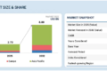
The hybrid bonding market has emerged as a cornerstone of next-generation semiconductor innovation. As the demand for faster, smaller, and more energy-efficient chips escalates, traditional packaging and interconnect technologies are reaching their physical limits. Hybrid bonding offers an advanced solution by enabling direct metal-to-metal and dielectric-to-dielectric connections at the nanoscale, supporting higher density, performance, and functionality in semiconductor devices. This market is critical because it directly impacts the development of 2.5D packaging, 3D stacked ICs, and other high-performance chip architectures that power AI, 5G, and next-generation computing.
Bonding Approaches: Wafer-to-Wafer, Die-to-Wafer, and Die-to-Die
The hybrid bonding market size is defined by three main approaches: wafer-to-wafer (W2W), die-to-wafer (D2W), and die-to-die (D2D). W2W bonding connects entire wafers directly, enabling high-volume, uniform integration suitable for large-scale manufacturing. D2W combines individual dies onto a wafer, offering flexibility in heterogeneous integration and allowing for mixed-technology designs. D2D bonding, the most granular approach, connects individual dies directly to each other, providing ultimate density and performance for highly specialized applications. Together, these bonding approaches form the foundation for advanced packaging solutions in the hybrid bonding ecosystem.
Essential Tools Driving the Market
The hybrid bonding market relies heavily on sophisticated equipment to ensure precision and yield. Wafer bonders provide accurate alignment and bonding pressure control, critical for nanoscale interconnects. Surface preparation tools ensure wafer and die surfaces are defect-free and optimized for bonding. Inspection and metrology tools verify alignment accuracy, surface planarity, and bond quality. Cleaning and CMP (Chemical Mechanical Planarization) systems remove contaminants and achieve ultra-flat surfaces, which are essential for reliable hybrid bonds. These tools collectively enable the scalability and reliability required for next-generation semiconductor applications.
Download PDF Brochure @ https://www.marketsandmarkets.com/pdfdownloadNew.asp?id=2641237
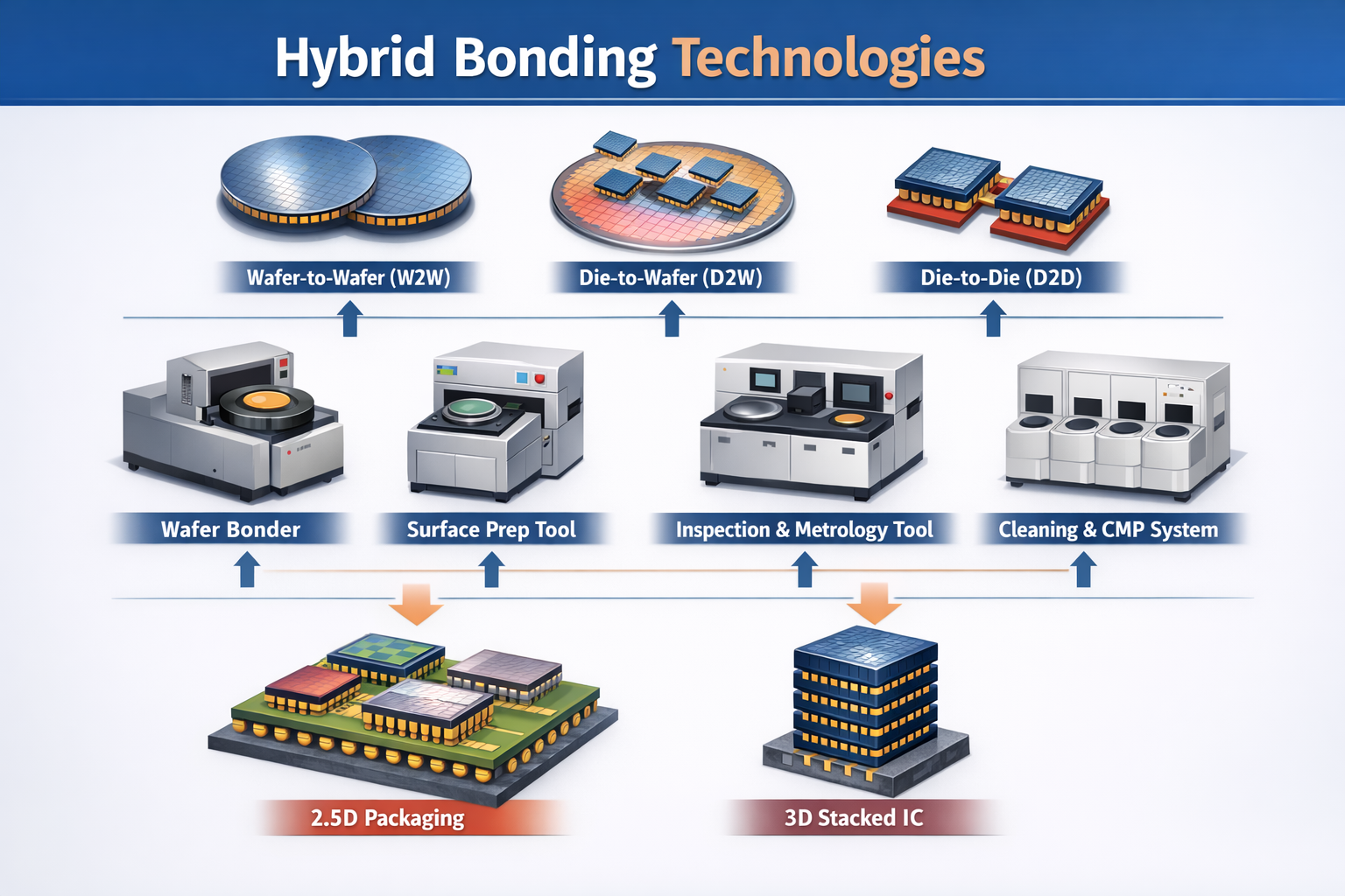
Advanced Packaging: 2.5D and 3D Stacked ICs
One of the most important drivers of the hybrid bonding market is its role in 2.5D packaging and 3D stacked ICs. In 2.5D packaging, multiple dies are placed on an interposer to increase performance while maintaining manageable thermal characteristics. Hybrid bonding enables high-density interconnections that allow for greater signal speed and lower power consumption compared to traditional wire bonding. In 3D stacked ICs, multiple layers of dies are vertically integrated, maximizing computational power in a minimal footprint. Hybrid bonding is the only viable method to reliably achieve such fine-pitch interconnects at scale, making it indispensable for cutting-edge chips used in AI accelerators, GPUs, and high-speed memory modules.
Why the Hybrid Bonding Market is Critical
The hybrid bonding market is central to semiconductor innovation because it addresses the limitations of conventional interconnects and enables technologies that are impossible with traditional packaging. It allows for increased transistor density, higher bandwidth, reduced power consumption, and more compact designs — all critical for next-generation applications. As industries push for AI-enabled devices, 5G infrastructure, autonomous vehicles, and advanced computing, hybrid bonding will remain a pivotal enabler, bridging the gap between wafer-level innovations and real-world high-performance chips.
Future hybrid bonding market Outlook
The future of the hybrid bonding market is closely tied to the evolution of semiconductor packaging and integration. With continued investment in wafer bonders, surface prep tools, CMP systems, and inspection technologies, the market will scale to meet the growing demand for 2.5D and 3D IC solutions. Emerging applications in AI, high-speed networking, and IoT devices will further accelerate adoption, solidifying the hybrid bonding market as a cornerstone of next-generation semiconductor innovation.
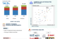
Key companies operating in the hybrid bonding market include EV Group (EVG) (Austria), Applied Materials, Inc. (US), SUSS MicroTec SE (Germany), Besi (Netherlands), Kulicke & Soffa Industries, Inc. (Singapore), Tokyo Electron (TEL) (Japan), and ASMPT (Singapore), among others.
FAQ: Hybrid Bonding Market
1. What is hybrid bonding in semiconductor manufacturing?
Hybrid bonding is an advanced packaging technology that enables direct metal-to-metal and dielectric-to-dielectric connections between wafers or dies. Unlike traditional solder-based interconnects, hybrid bonding allows ultra-fine pitch connections, improving performance, power efficiency, and integration density.
2. Why is the hybrid bonding market important for next-generation semiconductor innovation?
The hybrid bonding market is critical because it enables higher interconnect density, faster data transfer speeds, lower latency, and reduced power consumption. These capabilities are essential for AI processors, high-performance computing, 5G infrastructure, advanced memory solutions, and next-generation GPUs.
3. What are the main bonding approaches used in hybrid bonding?
The three primary approaches are Wafer-to-Wafer (W2W), Die-to-Wafer (D2W), and Die-to-Die (D2D). W2W is suitable for high-volume production, D2W supports heterogeneous integration, and D2D enables maximum design flexibility and ultra-high-density interconnections.
4. What equipment is required in the hybrid bonding process?
The process depends on advanced tools such as wafer bonders for precise alignment, surface preparation tools for defect-free bonding surfaces, inspection and metrology tools for quality verification, and cleaning and CMP (Chemical Mechanical Planarization) systems to achieve ultra-flat surfaces.
About MarketsandMarkets™
MarketsandMarkets™ has been recognized as one of America’s Best Management Consulting Firms by Forbes, as per their recent report.
MarketsandMarkets™ is a blue ocean alternative in growth consulting and program management, leveraging a man-machine offering to drive supernormal growth for progressive organizations in the B2B space. With the widest lens on emerging technologies, we are proficient in co-creating supernormal growth for clients across the globe.
Today, 80% of Fortune 2000 companies rely on MarketsandMarkets, and 90 of the top 100 companies in each sector trust us to accelerate their revenue growth. With a global clientele of over 13,000 organizations, we help businesses thrive in a disruptive ecosystem.
The B2B economy is witnessing the emergence of $25 trillion in new revenue streams that are replacing existing ones within this decade. We work with clients on growth programs, helping them monetize this $25 trillion opportunity through our service lines – TAM Expansion, Go-to-Market (GTM) Strategy to Execution, Market Share Gain, Account Enablement, and Thought Leadership Marketing.
Built on the ‘GIVE Growth’ principle, we collaborate with several Forbes Global 2000 B2B companies to keep them future-ready. Our insights and strategies are powered by industry experts, cutting-edge AI, and our Market Intelligence Cloud, KnowledgeStore™, which integrates research and provides ecosystem-wide visibility into revenue shifts.
To find out more, visit www.MarketsandMarkets™.com or follow us on Twitter , LinkedIn and Facebook .
Contact:
Mr. Rohan Salgarkar
MarketsandMarkets™ INC.
1615 South Congress Ave.
Suite 103, Delray Beach, FL 33445
USA: +1-888-600-6441