The semiconductor industry is entering a new era of innovation as traditional scaling approaches face increasing challenges in improving performance, power efficiency, and integration density. As demand for artificial intelligence (AI), high-performance computing (HPC), 5G, automotive electronics, and advanced memory solutions continues to rise, hybrid bonding technology is emerging as a critical enabler for next-generation semiconductor packaging.
The Hybrid Bonding Market is expected to experience significant growth through 2032, driven by increasing adoption of advanced packaging technologies, chiplet architectures, 3D stacked integrated circuits (3D ICs), and high-bandwidth memory (HBM). Hybrid bonding enables direct copper-to-copper and dielectric-to-dielectric connections, allowing semiconductor manufacturers to achieve higher interconnect density, improved electrical performance, and lower power consumption. The global hybrid bonding market is projected to reach USD 633.9 million by 2032 from USD 164.7 million in 2025, registering a CAGR of 21.2% from 2025 to 2032.
As the semiconductor ecosystem shifts from traditional transistor scaling toward heterogeneous integration, hybrid bonding is becoming a strategic technology for building future high-performance chips.
Understanding Hybrid Bonding Technology
Hybrid bonding is an advanced wafer-level and die-level bonding process that combines semiconductor components without traditional solder bumps or adhesives. The technology creates direct electrical and physical connections between semiconductor layers, enabling extremely fine-pitch interconnects.
Compared with conventional bonding methods, hybrid bonding offers:
- Higher interconnect density
- Improved signal performance
- Reduced power consumption
- Lower latency
- Better thermal performance
- Enhanced integration flexibility
These advantages make hybrid bonding particularly valuable for applications requiring massive data processing capabilities and compact semiconductor designs.
Market Segmentation
By Bonding Type
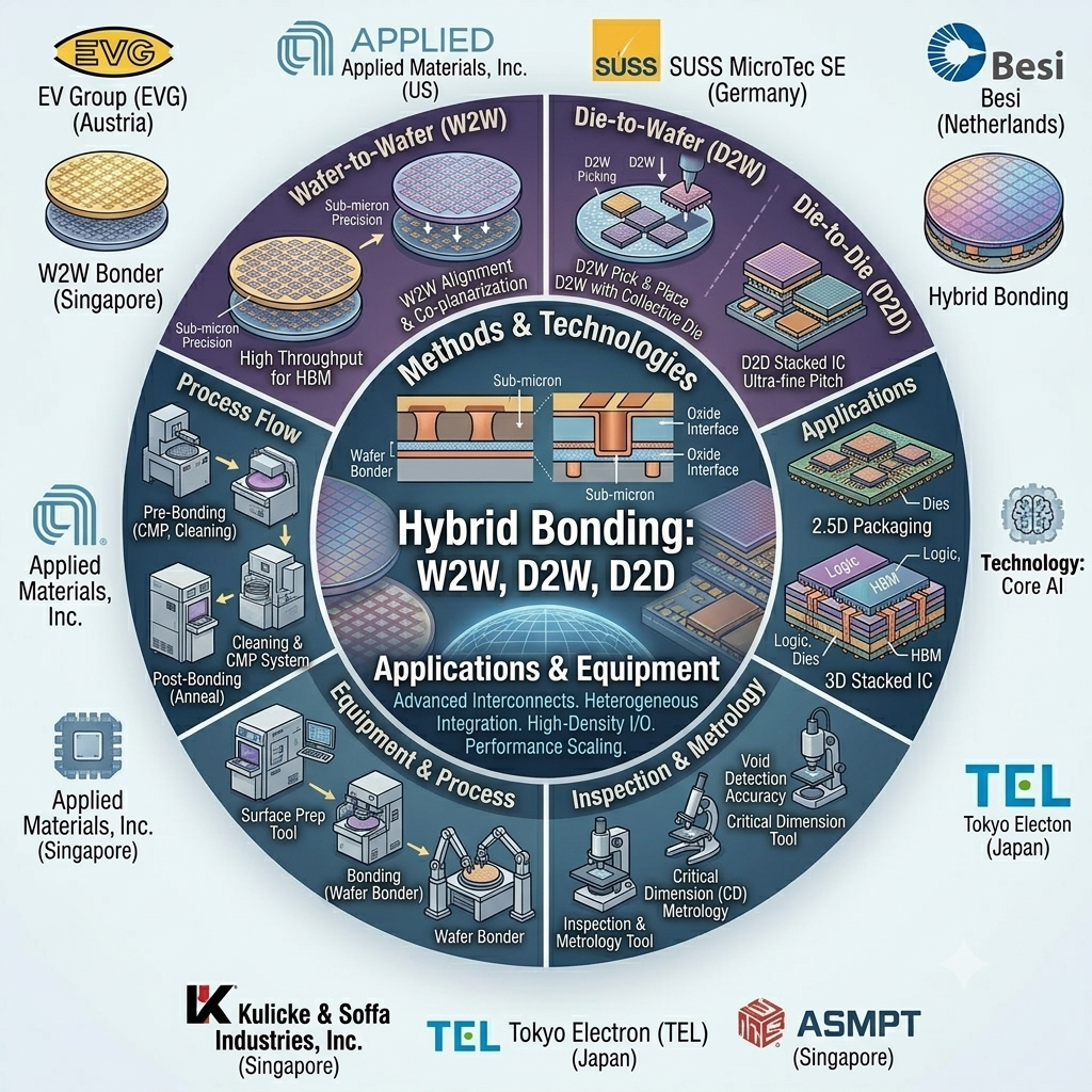
Wafer-to-Wafer (W2W)
Wafer-to-wafer bonding is widely used for applications requiring high-volume manufacturing and uniform wafer-level integration. It is particularly relevant for memory stacking and advanced image sensor applications.
Die-to-Wafer (D2W)
Die-to-wafer bonding enables integration of different semiconductor components, making it suitable for heterogeneous integration and chiplet-based architectures.
Die-to-Die (D2D)
Die-to-die bonding provides flexibility for advanced system designs by allowing individual chiplets or functional blocks to be integrated into a single package with high performance and scalability.
By Equipment
Wafer Bonder
Wafer bonders play a critical role in achieving precise alignment and reliable bonding between semiconductor layers. Increasing demand for advanced packaging is driving investments in high-accuracy bonding equipment.
Surface Preparation Tool
Surface preparation is essential for achieving defect-free hybrid bonding. Advanced cleaning and surface activation technologies improve bonding quality and manufacturing yield.
Inspection & Metrology Tool
Inspection and metrology systems help identify alignment errors, defects, and bonding inconsistencies. The growing complexity of semiconductor packages is increasing demand for advanced inspection solutions.
Cleaning & CMP System
Chemical mechanical polishing (CMP) and cleaning systems are essential for creating ultra-flat surfaces required for successful hybrid bonding processes.
By Application
2.5D Packaging
Hybrid bonding supports advanced 2.5D packaging architectures by enabling high-density connections between logic chips, memory modules, and specialized processing units.
The increasing demand for AI accelerators, GPUs, and networking processors is driving adoption of advanced packaging solutions.
3D Stacked IC
3D stacked IC technology represents one of the most promising applications for hybrid bonding. By stacking multiple semiconductor layers vertically, manufacturers can achieve higher performance while reducing footprint and power consumption.
Applications include:
- High-bandwidth memory (HBM)
- AI processors
- Data center chips
- Advanced sensors
- Mobile processors
Download PDF Brochure @ https://www.marketsandmarkets.com/pdfdownloadNew.asp?id=2641237
Key Market Growth Drivers
1. Rising Demand for AI and High-Performance Computing
The rapid expansion of generative AI, machine learning, and data-intensive applications is creating demand for powerful semiconductor architectures. AI processors require high bandwidth, low latency, and improved energy efficiency, making advanced packaging technologies essential.
Hybrid bonding enables closer integration between computing logic and memory components, supporting faster data transfer and improved system performance.
2. Growth of Chiplet-Based Architectures
Chiplets are transforming semiconductor design by allowing manufacturers to combine smaller functional blocks into customized high-performance packages.
Hybrid bonding provides the precision and density required for chiplet integration, enabling scalable designs that overcome the limitations of traditional monolithic chips.
3. Increasing Adoption of High-Bandwidth Memory (HBM)
The growth of AI workloads and data center applications is accelerating demand for HBM solutions. Hybrid bonding enables tighter memory stacking and improved interconnect performance, making it a key technology for future memory architectures.
4. Advancement of 3D IC Technology
As semiconductor manufacturers seek higher levels of integration, 3D IC architectures are becoming increasingly important. Hybrid bonding enables vertical stacking of chips while maintaining high electrical performance and reliability.
Emerging Market Trends
AI-Driven Semiconductor Packaging Innovation
AI applications are influencing semiconductor development by increasing demand for customized processors, advanced memory solutions, and high-performance packages. Hybrid bonding is expected to play an important role in enabling these next-generation designs.
Expansion of Advanced Packaging Capacity
Leading semiconductor manufacturers and packaging companies are increasing investments in advanced packaging facilities to support growing demand for AI chips, HPC processors, and advanced electronics.
Increasing Focus on Heterogeneous Integration
Heterogeneous integration allows different semiconductor technologies to be combined within a single package. Hybrid bonding provides the interconnect capability needed for integrating logic, memory, sensors, and specialized processors.
Improved Inspection and Manufacturing Precision
As bonding pitches become smaller, manufacturers are investing in advanced metrology, defect inspection, and process control technologies to improve yield and reliability.
Growing Adoption in Automotive Electronics
Automotive systems increasingly require advanced processors for autonomous driving, electric vehicles, and connected technologies. Hybrid bonding offers opportunities for high-performance automotive semiconductor solutions.
Growth Opportunities in the Hybrid Bonding Market
AI and Data Center Infrastructure
The expansion of AI servers and cloud computing infrastructure is creating significant opportunities for advanced semiconductor packaging technologies.
Next-Generation Memory Technologies
The increasing demand for faster and higher-capacity memory solutions will continue driving hybrid bonding adoption in HBM and stacked memory applications.
Semiconductor Manufacturing Equipment
Equipment manufacturers specializing in bonding, inspection, metrology, CMP, and surface preparation are positioned to benefit from rising investments in hybrid bonding production capabilities.
Advanced Consumer Electronics
Compact, powerful consumer devices require improved semiconductor integration. Hybrid bonding can support smaller form factors while delivering enhanced performance.
Challenges Impacting Market Growth
Despite strong growth potential, hybrid bonding adoption faces several challenges:
- High equipment and manufacturing costs
- Complex process requirements
- Need for advanced alignment accuracy
- Yield management challenges
- Limited manufacturing ecosystem compared with traditional packaging methods
However, continuous innovation in materials, equipment, and manufacturing processes is expected to improve scalability and cost efficiency.
Future Outlook
The Hybrid Bonding Market through 2032 is expected to expand significantly as semiconductor manufacturers increasingly adopt advanced packaging strategies to meet growing performance demands.
The convergence of AI, cloud computing, chiplets, HBM, and 3D IC technologies will continue driving demand for high-density integration solutions. Hybrid bonding will become a foundational technology for future semiconductor architectures by enabling faster, smaller, and more energy-efficient electronic systems.
Hybrid bonding is redefining semiconductor packaging by enabling unprecedented levels of integration, performance, and efficiency. As the industry moves beyond traditional scaling and embraces heterogeneous integration, hybrid bonding will play a central role in supporting advanced computing, AI, memory, and electronic applications.
With increasing investments in 2.5D packaging, 3D stacked ICs, and next-generation semiconductor manufacturing, the Hybrid Bonding Market is positioned for strong growth through 2032, creating significant opportunities across the semiconductor value chain.
Frequently Asked Questions (FAQs) – Hybrid Bonding Market
1. What is the projected growth outlook for the Hybrid Bonding Market by 2032?
The Hybrid Bonding Market is expected to witness significant growth through 2032, driven by increasing demand for advanced semiconductor packaging, artificial intelligence (AI) processors, high-performance computing (HPC), chiplet architectures, and 3D stacked integrated circuits (3D ICs).
2. What is hybrid bonding technology, and why is it important for semiconductors?
Hybrid bonding is an advanced semiconductor packaging technology that creates direct connections between semiconductor layers using dielectric-to-dielectric and copper-to-copper bonding. It enables higher interconnect density, improved electrical performance, lower power consumption, and greater integration compared with traditional packaging methods.
3. What factors are driving the growth of the Hybrid Bonding Market?
Key growth drivers include:
- Increasing adoption of AI and high-performance computing applications
- Rising demand for high-bandwidth memory (HBM)
- Growth of chiplet-based semiconductor architectures
- Expansion of 2.5D and 3D IC packaging technologies
- Increasing investments in advanced semiconductor manufacturing
- Demand for smaller, faster, and more energy-efficient electronic devices
4. What are the major types of hybrid bonding technologies?
The Hybrid Bonding Market is segmented into:
- Wafer-to-Wafer (W2W): Used for high-volume wafer-level integration applications.
- Die-to-Wafer (D2W): Enables integration of individual dies onto wafers for heterogeneous semiconductor designs.
- Die-to-Die (D2D): Supports flexible chiplet integration and advanced multi-die architectures.
5. What are the key applications of hybrid bonding technology?
Major applications include:
- 2.5D packaging
- 3D stacked ICs
- High-bandwidth memory (HBM)
- AI accelerators
- Data center processors
- Advanced sensors
- Automotive semiconductor solutions
6. How is hybrid bonding supporting AI and high-performance computing?
AI and HPC workloads require processors with higher bandwidth, lower latency, and improved energy efficiency. Hybrid bonding enables closer integration of logic and memory components, allowing semiconductor manufacturers to develop high-performance chips capable of handling complex computational workloads.
7. Which equipment is used in hybrid bonding processes?
Key equipment involved in hybrid bonding includes:
- Wafer bonders
- Surface preparation tools
- Inspection and metrology tools
- Cleaning and chemical mechanical polishing (CMP) systems
These systems help achieve precise alignment, defect reduction, and high manufacturing yields.
About MarketsandMarkets™
MarketsandMarkets™ provides quantified B2B research on 30,000 high growth niche opportunities/threats which will impact 70% to 80% of worldwide companies’ revenues. Currently servicing 7500 customers worldwide including 80% of global Fortune 1000 companies as clients. Almost 75,000 top officers across eight industries worldwide approach MarketsandMarkets™ for their painpoints around revenues decisions.
Our 850 fulltime analyst and SMEs at MarketsandMarkets™ are tracking global high growth markets following the “Growth Engagement Model – GEM”. The GEM aims at proactive collaboration with the clients to identify new opportunities, identify most important customers, write “Attack, avoid and defend” strategies, identify sources of incremental revenues for both the company and its competitors. MarketsandMarkets™ now coming up with 1,500 MicroQuadrants (Positioning top players across leaders, emerging companies, innovators, strategic players) annually in high growth emerging segments. MarketsandMarkets™ is determined to benefit more than 10,000 companies this year for their revenue planning and help them take their innovations/disruptions early to the market by providing them research ahead of the curve.
MarketsandMarkets’s flagship competitive intelligence and market research platform, “Knowledgestore” connects over 200,000 markets and entire value chains for deeper understanding of the unmet insights along with market sizing and forecasts of niche markets.
Contact:
Mr. Rohan Salgarkar
MarketsandMarkets™ INC.
630 Dundee Road
Suite 430
Northbrook, IL 60062
USA : 1-888-600-6441
