The semiconductor industry is entering a new era of innovation where traditional transistor scaling alone can no longer meet the performance requirements of artificial intelligence (AI), high-performance computing (HPC), advanced memory, and next-generation mobile devices. As chipmakers seek higher bandwidth, lower latency, improved power efficiency, and greater interconnect density, advanced packaging technologies have become a strategic priority.
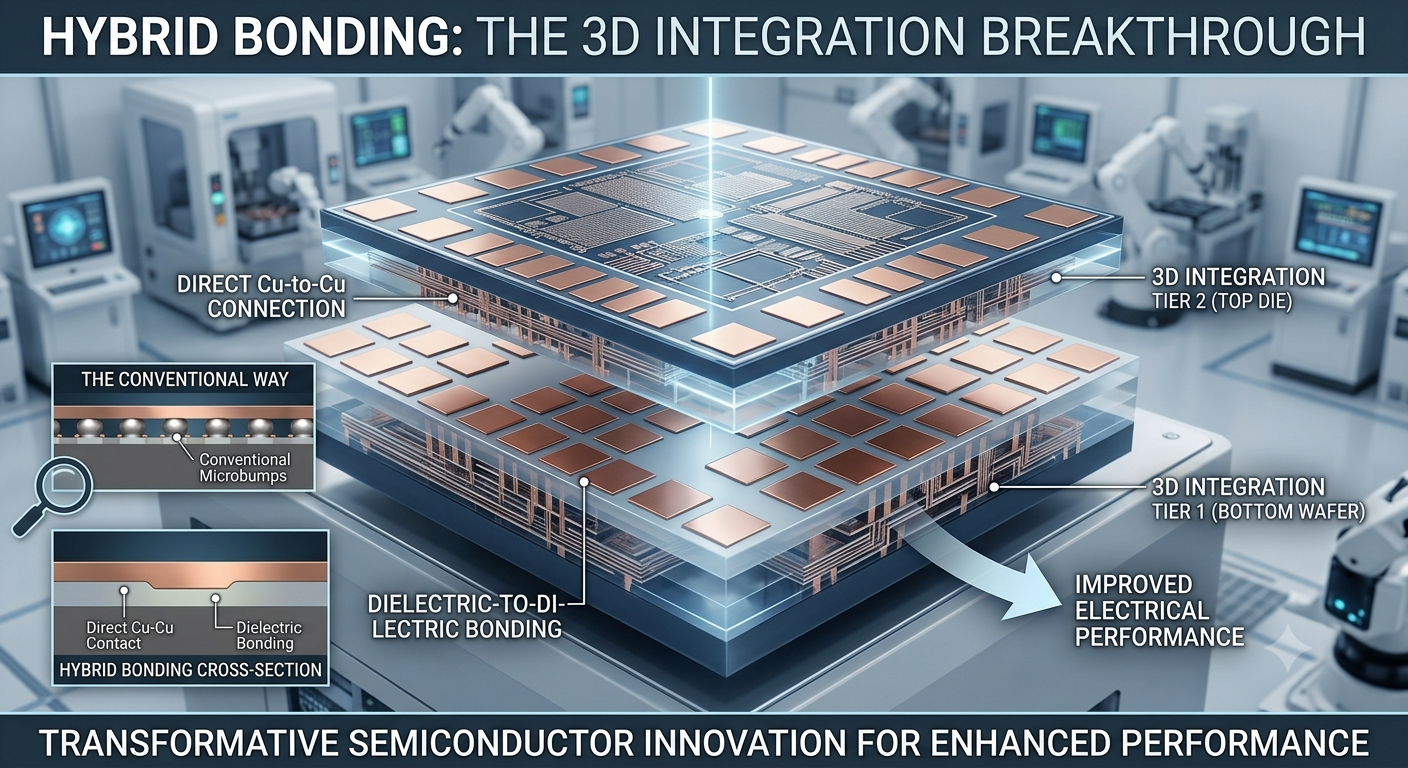
Among these technologies, hybrid bonding has emerged as one of the most transformative innovations in semiconductor manufacturing. By enabling direct copper-to-copper and dielectric-to-dielectric connections without conventional microbumps, hybrid bonding delivers significantly improved electrical performance and supports the industry’s transition toward three-dimensional (3D) integration.
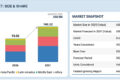
According to MarketsandMarkets, The global hybrid bonding market is projected to reach USD 633.9 million by 2032 from USD 164.7 million in 2025, registering a CAGR of 21.2% from 2025 to 2032. This rapid expansion reflects growing demand for advanced packaging solutions capable of supporting AI processors, chiplet architectures, memory stacking, and heterogeneous integration.
As semiconductor manufacturers continue to push beyond Moore’s Law, hybrid bonding is becoming a foundational technology shaping the future of chip design and manufacturing.
Understanding Hybrid Bonding Technology
Hybrid bonding is an advanced semiconductor packaging process that directly connects wafers or dies through simultaneous dielectric and metal bonding.
Unlike traditional packaging approaches that rely on solder bumps, hybrid bonding offers:
- Ultra-fine pitch interconnects
- Higher input/output density
- Lower power consumption
- Reduced signal loss
- Improved thermal performance
- Enhanced system integration
These advantages make hybrid bonding particularly attractive for applications requiring extreme computational performance and energy efficiency.
The technology is increasingly being deployed across:
- High-bandwidth memory (HBM)
- AI accelerators
- Data center processors
- Mobile chipsets
- Image sensors
- Advanced logic devices
- Heterogeneous integration platforms
Hybrid Bonding Market Growth Accelerates Amid Major Semiconductor Industry Shifts
Several structural shifts are fueling the rapid growth of the Hybrid Bonding Market.
End of Traditional Scaling Advantages
For decades, semiconductor innovation was driven primarily by transistor miniaturization. However, as process nodes become increasingly complex and expensive, manufacturers are turning toward advanced packaging technologies to continue improving performance.
Hybrid bonding enables system-level scaling by allowing multiple dies to function as a unified computing platform.
AI Infrastructure Expansion
Artificial intelligence workloads require unprecedented processing power and memory bandwidth.
Modern AI accelerators depend on:
- High-speed memory access
- Dense interconnect architectures
- Low-power operation
- Reduced latency
Hybrid bonding addresses these requirements by creating ultra-short interconnect pathways between processing units and memory devices. This capability is becoming essential for AI infrastructure development.
Growth of High-Performance Computing
HPC applications continue expanding across scientific research, cloud computing, financial modeling, and defense systems.
As computational complexity increases, hybrid bonding enables advanced processor architectures capable of delivering greater performance without significantly increasing power consumption.
Download PDF Brochure @ https://www.marketsandmarkets.com/pdfdownloadNew.asp?id=2641237
Core Equipment Dominance in the Hybrid Bonding Market
A defining characteristic of the Hybrid Bonding Market is the critical role played by specialized equipment vendors.
Unlike many semiconductor technologies, successful hybrid bonding requires exceptional process precision, making equipment capabilities a major competitive differentiator.
Wafer Bonders: The Dominant Equipment Segment
According to MarketsandMarkets, wafer bonders represented the largest equipment segment and continue to dominate the market due to their ability to support high-volume wafer-to-wafer (W2W) manufacturing.
Wafer bonders provide:
- Precise alignment accuracy
- High process uniformity
- Enhanced production throughput
- Improved manufacturing yield
- Reduced process variation
These characteristics make them indispensable for advanced memory, CMOS image sensor (CIS), and 3D logic production.
As foundries and integrated device manufacturers (IDMs) expand advanced packaging capacity, demand for wafer bonding systems is expected to increase significantly.
Surface Preparation and Cleaning Systems
Successful hybrid bonding depends heavily on surface quality.
Advanced surface preparation systems ensure:
- Particle-free interfaces
- Optimal wafer flatness
- Enhanced bonding strength
- Improved electrical performance
Cleaning systems, plasma activation tools, and chemical mechanical polishing (CMP) equipment have therefore become essential components of hybrid bonding production lines.
Inspection and Metrology Tools
As interconnect dimensions continue shrinking, manufacturers require increasingly sophisticated metrology solutions.
Inspection systems help ensure:
- Bond alignment accuracy
- Surface quality verification
- Defect detection
- Yield optimization
Growing investments in advanced metrology technologies are strengthening the broader hybrid bonding ecosystem.
Key Drivers Powering the Rapid Expansion of the Hybrid Bonding Market
AI and Machine Learning Demand
The AI revolution is one of the strongest growth catalysts for the Hybrid Bonding Market.
AI training and inference systems require:
- Massive memory bandwidth
- High-speed communication pathways
- Efficient power utilization
Hybrid bonding enables these capabilities while supporting compact and scalable architectures.
Chiplet-Based Design Adoption
The semiconductor industry is increasingly embracing chiplet architectures.
Rather than manufacturing a single monolithic chip, chiplets allow multiple specialized dies to be integrated into one package.
Benefits include:
- Improved manufacturing yields
- Lower production costs
- Greater design flexibility
- Faster product development cycles
Hybrid bonding serves as a key enabling technology for chiplet integration.
Advanced Memory Requirements
High-bandwidth memory solutions increasingly rely on vertically stacked architectures.
Hybrid bonding supports:
- Dense memory stacking
- Reduced signal delays
- Improved energy efficiency
- Enhanced system performance
As AI systems demand larger memory capacities, hybrid bonding adoption is expected to accelerate.
Technology Trends Reshaping Semiconductor Manufacturing
Transition Toward 3D IC Integration
One of the most significant trends in the Hybrid Bonding Market is the move toward 3D integrated circuits.
3D IC architectures provide:
- Greater transistor density
- Improved performance
- Reduced package footprint
- Enhanced energy efficiency
MarketsandMarkets identifies the industry’s transition toward 3D integration as a primary market driver.
Heterogeneous Integration Emerges as a Growth Engine
Heterogeneous integration is projected to be the fastest-growing segment during the forecast period.
This approach combines:
- Logic processors
- Memory components
- RF modules
- Analog devices
- AI accelerators
into a single integrated package.
Hybrid bonding provides the dense interconnect structures required to make heterogeneous integration commercially viable.
Copper-to-Copper Bonding Leadership
Copper-to-copper (Cu-Cu) bonding continues to gain momentum due to its superior electrical characteristics.
Advantages include:
- Lower resistance
- Higher signal integrity
- Improved thermal conductivity
- Greater interconnect density
These benefits make Cu-Cu bonding particularly attractive for advanced AI and HPC applications.
Competitive Landscape: Equipment Leaders Driving Innovation
The Hybrid Bonding Market is characterized by a relatively concentrated competitive landscape dominated by specialized equipment manufacturers.
Leading companies include:
- EV Group (EVG)
- Applied Materials
- SUSS MicroTec
- Besi
- Kulicke & Soffa
- Tokyo Electron (TEL)
- ASMPT
These organizations continue investing heavily in:
- Alignment precision
- Automation technologies
- Throughput optimization
- Yield improvement
- Process control solutions
MarketsandMarkets identifies EV Group, SUSS MicroTec, and Applied Materials among the leading players with strong market presence and technology portfolios.
Competition increasingly revolves around the ability to deliver scalable solutions capable of supporting high-volume manufacturing environments.
Regional Dynamics
Asia Pacific Leads Global Adoption
Asia Pacific accounted for over half of global market revenue and remains the dominant region in the Hybrid Bonding Market.
The region benefits from:
- Large semiconductor manufacturing capacity
- Strong foundry ecosystems
- Government support programs
- Growing advanced packaging investments
China’s Strategic Expansion
China is expected to maintain a leading position due to substantial investments in:
- Advanced packaging facilities
- Domestic semiconductor manufacturing
- Equipment localization initiatives
- AI infrastructure development
The country’s emphasis on semiconductor self-sufficiency is creating significant opportunities for hybrid bonding adoption.
Challenges Facing the Hybrid Bonding Market
Despite strong growth prospects, several challenges remain.
High Capital Requirements
Hybrid bonding production lines require substantial investments in:
- Wafer bonders
- Metrology systems
- Surface preparation equipment
- Process automation solutions
Manufacturing Complexity
Achieving reliable hybrid bonding requires extremely tight process control and precision manufacturing.
Even minor variations can affect:
- Yield performance
- Reliability
- Electrical characteristics
Supply Chain Constraints
As demand increases, manufacturers must scale production while maintaining quality and consistency across increasingly complex semiconductor supply chains.
Future Outlook: The Next Phase of Hybrid Bonding Evolution
The future of the Hybrid Bonding Market appears exceptionally strong.
Several trends will shape market development through 2032:
- Expansion of AI infrastructure
- Growth of chiplet architectures
- Increased memory stacking adoption
- Wider deployment of heterogeneous integration
- Continued 3D IC commercialization
- Advanced packaging investments by foundries and IDMs
As semiconductor innovation increasingly shifts from transistor scaling toward system-level integration, hybrid bonding will become one of the industry’s most important enabling technologies.
Conclusion
The Hybrid Bonding Market is rapidly transitioning from an emerging packaging technology to a critical pillar of advanced semiconductor manufacturing. Driven by AI, HPC, memory stacking, chiplet architectures, and 3D integration, the market is positioned for substantial growth over the coming decade.
Core equipment categories—particularly wafer bonders, surface preparation systems, and metrology tools—will remain central to this evolution. As semiconductor manufacturers pursue greater performance, efficiency, and integration density, hybrid bonding is expected to play a defining role in the future of advanced packaging and next-generation chip architectures.
With the market projected to grow at a CAGR of 21.2% through 2032, hybrid bonding is no longer simply an innovation opportunity—it is becoming a strategic necessity for semiconductor competitiveness in the AI era.
About MarketsandMarkets™
MarketsandMarkets™ has been recognized as one of America’s Best Management Consulting Firms by Forbes, as per their recent report.
MarketsandMarkets™ is a blue ocean alternative in growth consulting and program management, leveraging a man-machine offering to drive supernormal growth for progressive organizations in the B2B space. With the widest lens on emerging technologies, we are proficient in co-creating supernormal growth for clients across the globe.
Today, 80% of Fortune 2000 companies rely on MarketsandMarkets, and 90 of the top 100 companies in each sector trust us to accelerate their revenue growth. With a global clientele of over 13,000 organizations, we help businesses thrive in a disruptive ecosystem.
The B2B economy is witnessing the emergence of $25 trillion in new revenue streams that are replacing existing ones within this decade. We work with clients on growth programs, helping them monetize this $25 trillion opportunity through our service lines – TAM Expansion, Go-to-Market (GTM) Strategy to Execution, Market Share Gain, Account Enablement, and Thought Leadership Marketing.
Built on the ‘GIVE Growth’ principle, we collaborate with several Forbes Global 2000 B2B companies to keep them future-ready. Our insights and strategies are powered by industry experts, cutting-edge AI, and our Market Intelligence Cloud, KnowledgeStore™, which integrates research and provides ecosystem-wide visibility into revenue shifts.
To find out more, visit www.MarketsandMarkets™.com or follow us on Twitter , LinkedIn and Facebook .
Contact:
Mr. Rohan Salgarkar
MarketsandMarkets™ INC.
1615 South Congress Ave.
Suite 103, Delray Beach, FL 33445
USA: +1-888-600-6441